74ALVCH162827DGG Overview
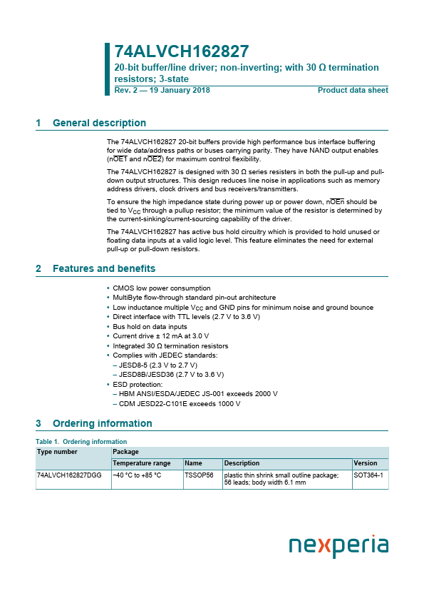
The 74ALVCH162827 20-bit buffers provide high performance bus interface buffering for wide data/address paths or buses carrying parity. They have NAND output enables (nOE1 and nOE2) for maximum control flexibility. The 74ALVCH162827 is designed with 30 Ω series resisters in both the pull-up and pulldown output structures.
74ALVCH162827DGG Key Features
- CMOS low power consumption
- MultiByte flow-through standard pin-out architecture
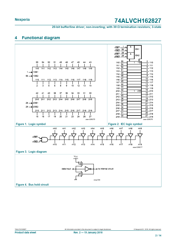
- Low inductance multiple VCC and GND pins for minimum noise and ground bounce
- Direct interface with TTL levels (2.7 V to 3.6 V)
- Bus hold on data inputs
- Current drive ± 12 mA at 3.0 V
- Integrated 30 Ω termination resistors
- plies with JEDEC standards
- JESD8-5 (2.3 V to 2.7 V)
- JESD8B/JESD36 (2.7 V to 3.6 V)