Datasheet4U Logo Datasheet4U.com

74HCT367D - Hex buffer/line driver

Download the 74HCT367D datasheet PDF (74HC367 included). The manufacturer datasheet provides complete specifications, pinout details, electrical characteristics, and typical applications for hex buffer/line driver.

Description

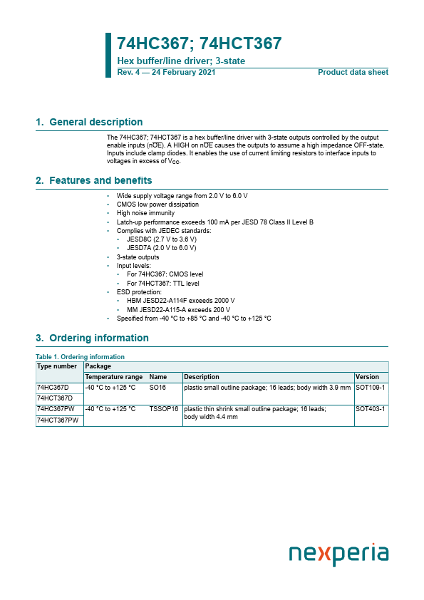
The 74HC367; 74HCT367 is a hex buffer/line driver with 3-state outputs controlled by the output enable inputs (nOE).

A HIGH on nOE causes the outputs to assume a high impedance OFF-state.

Inputs include clamp diodes.

Features

  • Wide supply voltage range from 2.0 V to 6.0 V.
  • CMOS low power dissipation.
  • High noise immunity.
  • Latch-up performance exceeds 100 mA per JESD 78 Class II Level B.
  • Complies with JEDEC standards:.
  • JESD8C (2.7 V to 3.6 V).
  • JESD7A (2.0 V to 6.0 V).
  • 3-state outputs.
  • Input levels:.
  • For 74HC367: CMOS level.
  • For 74HCT367: TTL level.
  • ESD protection:.
  • HBM JESD22-A114F exceeds 2000 V.

📥 Download Datasheet

Note: The manufacturer provides a single datasheet file (74HC367-nexperia.pdf) that lists specifications for multiple related part numbers.
Other Datasheets by nexperia

Full PDF Text Transcription

Click to expand full text
74HC367; 74HCT367 Hex buffer/line driver; 3-state Rev. 4 — 24 February 2021 Product data sheet 1. General description The 74HC367; 74HCT367 is a hex buffer/line driver with 3-state outputs controlled by the output enable inputs (nOE). A HIGH on nOE causes the outputs to assume a high impedance OFF-state. Inputs include clamp diodes. It enables the use of current limiting resistors to interface inputs to voltages in excess of VCC. 2. Features and benefits • Wide supply voltage range from 2.0 V to 6.0 V • CMOS low power dissipation • High noise immunity • Latch-up performance exceeds 100 mA per JESD 78 Class II Level B • Complies with JEDEC standards: • JESD8C (2.7 V to 3.6 V) • JESD7A (2.0 V to 6.
Published: |