onsemi FDY1002PZ
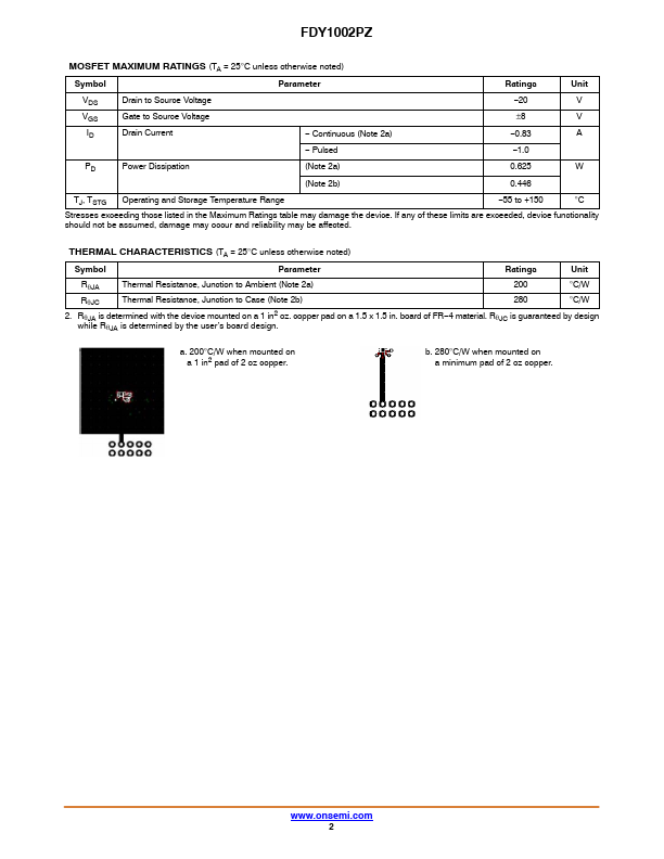
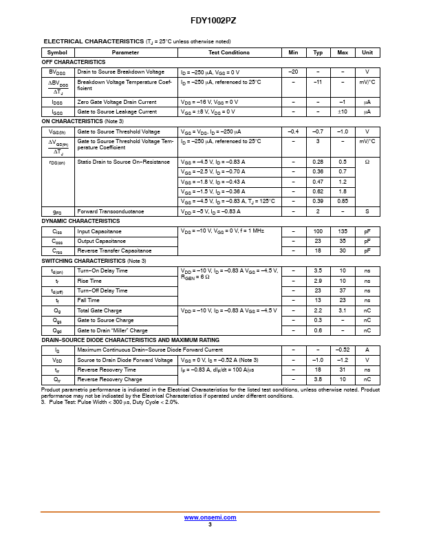
This Dual P−Channel MOSFET has been designed using onsemi’s advanced Power Trench process to optimize the rDS(on) @ VGS = –1.5 V. The diode connected between the gate and source serves only as protection against ESD.| Part No. | FDY1002PZ |
|---|---|
| Datasheet | FDY1002PZ Download |
| Manufacturer |  onsemi |
| Description | Dual P-Channel MOSFET |
| Buy | Stock & Price |
GENERAL DESCRIPTION
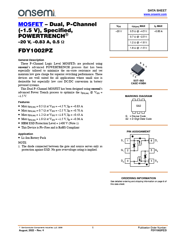
These P−Channel Logic Level MOSFETs are produced using onsemi’s advanced POWERTRENCH process that has been especially tailored to minimize the on−state resistance and yet maintain low gate charge for superior switching performance. These devices are well suited for all applications where small size is desireable but especially low cost DC/DC conversion in battery powered systems.FEATURES
● Max rDS(on) = 0.5 W at VGS = –4.5 V, ID = –0.83 A● Max rDS(on) = 0.7 W at VGS = –2.5 V, ID = –0.70 A
● Max rDS(on) = 1.2 W at VGS = –1.8 V, ID = –0.43 A
● Max rDS(on) = 1.8 W at VGS = –1.5 V, ID = –0.36 A
● HBM ESD Protection Level = 1400 V (Note 1)
● This Device is Pb−Free and is RoHS Compliant Application
● Li−Ion Battery Pack NOTE: 1. No gate overvoltage rating is implied. DATA SHEET VDS −20 V rDS(on) MAX 0.5 W @ −4.5 V 0.7 W @ −2.5 V 1.2 W @ −1.8 V 1.8 W @ −1.5 V ID MAX −0.83 A 6 5 4 1 23 SOT−563 CASE 419BH MARKING DIAGRAM G&2 G = Device Code &2 = 2−Digit Date Code PIN ASSIG...