Datasheet4U Logo Datasheet4U.com

US5D308 - 8-Output Ultra-Low Additive Jitter Differential Clock Buffer/Level Translator

Description

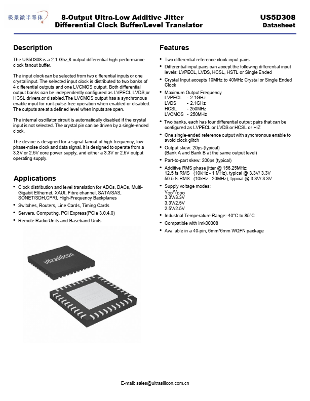
The US5D308 is a 2.1-Ghz,8-output differential high-performance clock fanout buffer.

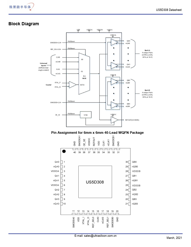
The input clock can be selected from two differential inputs or one crystal input.

The selected input clock is distributed to two banks of 4 differential outputs and one LVCMOS output.

Features

  • Two differential reference clock input pairs.
  • Differential input pairs can accept the following differential input levels: LVPECL, LVDS, HCSL, HSTL or Single Ended.
  • Crystal Input accepts 10MHz to 40MHz Crystal or Single Ended Clock.
  • Maximum Output Frequency LVPECL - 2.1GHz LVDS - 2.1GHz HCSL - 250MHz LVCMOS - 250MHz.
  • Two banks, each has four differential output pairs that can be configured as LVPECL or LVDS or HCSL or HiZ.
  • One single-ended r.

📥 Download Datasheet

Datasheet Details

Part number US5D308
Manufacturer ultrasilicon
File Size 912.42 KB
Description 8-Output Ultra-Low Additive Jitter Differential Clock Buffer/Level Translator
Datasheet download datasheet US5D308 Datasheet

Full PDF Text Transcription

Click to expand full text
8-Output Ultra-Low Additive Jitter Differential Clock Buffer/Level Translator US5D308 Datasheet Description The US5D308 is a 2.1-Ghz,8-output differential high-performance clock fanout buffer. The input clock can be selected from two differential inputs or one crystal input. The selected input clock is distributed to two banks of 4 differential outputs and one LVCMOS output. Both differential output banks can be independently configured as LVPECL,LVDS,or HCSL drivers,or disabled.The LVCMOS output has a synchronous enable input for runt-pulse-free operation when enabled or disabled. The outputs are at a defined level when inputs are open. The internal oscillator circuit is automatically disabled if the crystal input is not selected. The crystal pin can be driven by a single-ended clock.
Published: |