Description
6
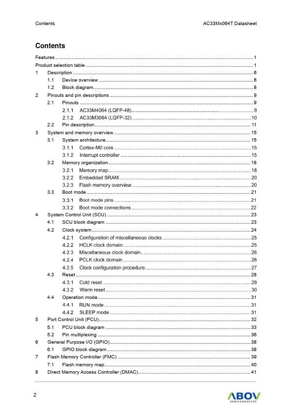
1.1 Device overview 6 1.2 Block diagram 8 2 Pinouts and pin descriptions 9 2.1 Pinouts 9
2.2 Pin description 11 3 System and memory overview 15
3.1 System architecture 15
3.2 Memory organization 18
3.3 Boot mode 21
4 System Control Unit (SCU) 23 4.1 SCU block diagram 23 4.2 Clock system 24
4.3 Reset 28
4.4 Operation mode 31
5 Port Control Unit (PCU) 32 5.1 PCU block diagram 33 5.2 Pin multiplexing 36
6 General Purpose I/O (GPIO) 38 6.1 GPIO block diagram 38
7 Flash Memory Cont
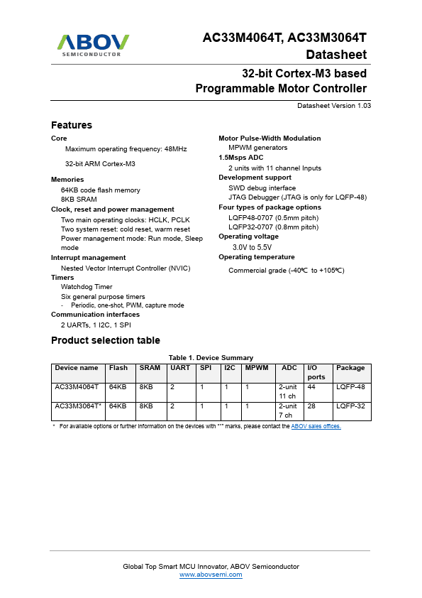
Features
- Core Maximum operating frequency: 48MHz
32-bit ARM Cortex-M3
Memories 64KB code flash memory 8KB SRAM
Clock, reset and power management Two main operating clocks: HCLK, PCLK Two system reset: cold reset, warm reset Power management mode: Run mode, Sleep mode
Interrupt management Nested Vector Interrupt Controller (NVIC)
Timers Watchdog Timer Six general purpose timers - Periodic, one-shot, PWM, capture mode
Communication interfaces 2 UARTs, 1 I2C, 1 SPI
Product selection table
Motor Pulse-Width.


