Datasheet Details
| Part number | ADN4668 |
|---|---|
| Manufacturer | Analog Devices |
| File Size | 423.63 KB |
| Description | 3V LVDS Quad CMOS Differential Line Receiver |
| Datasheet |
 ADN4668 Datasheet ADN4668 Datasheet
|
|
|
| Part number | ADN4668 |
|---|---|
| Manufacturer | Analog Devices |
| File Size | 423.63 KB |
| Description | 3V LVDS Quad CMOS Differential Line Receiver |
| Datasheet |
ADN4668 Datasheet
|
|
|
|
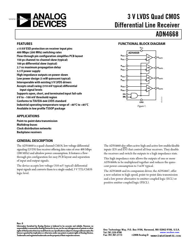
The ADN4668 is a quad-channel CMOS, low voltage differential signaling (LVDS) line receiver offering data rates of over 400 Mbps (200 MHz) and ultralow power consumption.
📁 Similar Datasheet