Datasheet Details
| Part number | ADP1196 |
|---|---|
| Manufacturer | Analog Devices |
| File Size | 368.25 KB |
| Description | High-Side or Low-Side Load Switch |
| Datasheet |
 ADP1196_AnalogDevices.pdf ADP1196_AnalogDevices.pdf
|
|
|
The ADP1196 by Analog Devices is a High-Side or Low-Side Load Switch. Below is the official datasheet preview.
| Part number | ADP1196 |
|---|---|
| Manufacturer | Analog Devices |
| File Size | 368.25 KB |
| Description | High-Side or Low-Side Load Switch |
| Datasheet |
ADP1196_AnalogDevices.pdf
|
|
|
|
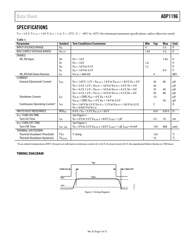
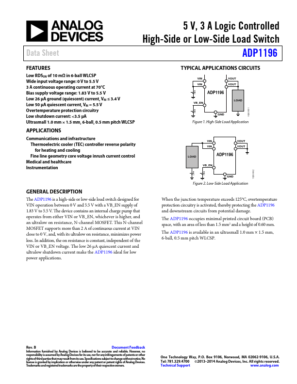
The ADP1196 is a high-side or low-side load switch designed for VIN operation between 0 V and 5.5 V with a VB_EN supply of 1.83 V to 5.5 V.
📁 ADP1196 Similar Datasheet