Datasheet Details
| Part number | ADP3654 |
|---|---|
| Manufacturer | Analog Devices |
| File Size | 343.52 KB |
| Description | 4A MOSFET Driver |
| Datasheet |
 ADP3654-AnalogDevices.pdf ADP3654-AnalogDevices.pdf
|
|
|
The ADP3654 by Analog Devices is a 4A MOSFET Driver. Below is the official datasheet preview.
| Part number | ADP3654 |
|---|---|
| Manufacturer | Analog Devices |
| File Size | 343.52 KB |
| Description | 4A MOSFET Driver |
| Datasheet |
ADP3654-AnalogDevices.pdf
|
|
|
|
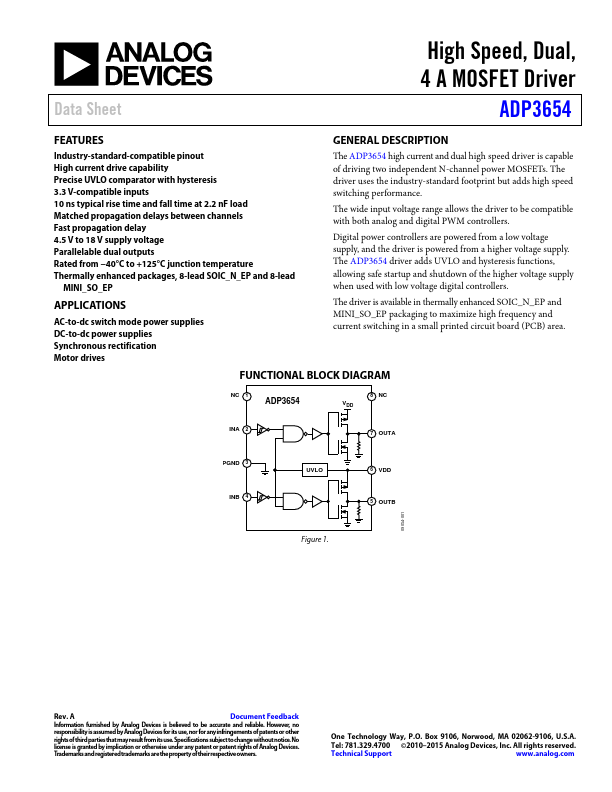
Industry-standard-compatible pinout High current drive capability Precise UVLO comparator with hysteresis 3.3 V-compatible inputs 10 ns typical rise time and fall time at 2.2 nF load Matched propagation delays between channels Fast propagation delay 4.5 V to 18 V supply voltage Parallelable dual outputs Rated from 40°C to +125°C junction temperature Thermally enhanced packages, 8-lead SOIC_N_EP and 8-lead MINI_SO_EP APPLICATIONS AC-to-dc switch mode power supplies DC-to-dc power suppli
📁 ADP3654 Similar Datasheet