Click to expand full text
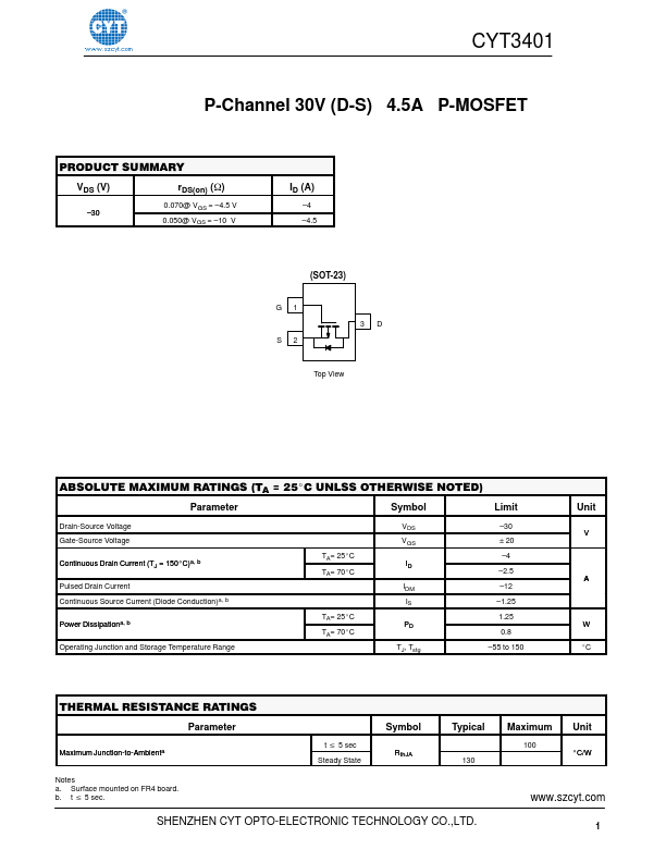
CYT3401
P-Channel 30V (D-S) 4.5A P-MOSFET
PRODUCT SUMMARY
VDS (V)
rDS(on) (W)
0.070@ VGS = –4.5 V –30
0.050@ VGS = –10 V
ID (A)
–4 –4.5
T (SOT-23)
G1 S2
3D
Top View Si2307DS (A7)* *Marking Code
ABSOLUTE MAXIMUM RATINGS (TA = 25_C UNLSS OTHERWISE NOTED)
Parameter
Symbol
Limit
Drain-Source Voltage Gate-Source Voltage Continuous Drain Current (TJ = 150_C)a, b Pulsed Drain Current Continuous Source Current (Diode Conduction)a, b Power Dissipationa, b
Operating Junction and Storage Temperature Range
TA= 25_C TA= 70_C
TA= 25_C TA= 70_C
VDS VGS ID IDM
IS PD TJ, Tstg
–30 "20 –4 –2.5 –12 –1.25 1.25 0.8 –55 to 150
Unit
V
A
W _C
THERMAL RESISTANCE RATINGS Parameter
Maximum Junction-to-Ambienta
t v 5 sec Steady State
Symbol
RthJA
Typical
130
Maximum
100
Unit
_C/W
Notes a.
 CYT3401 Datasheet