Datasheet Details
| Part number | CY5057 |
|---|---|
| Manufacturer | Cypress Semiconductor |
| File Size | 297.30 KB |
| Description | High-Frequency Flash Programmable PLL Die |
| Datasheet |
 CY5057_CypressSemiconductor.pdf CY5057_CypressSemiconductor.pdf
|
| Part number | CY5057 |
|---|---|
| Manufacturer | Cypress Semiconductor |
| File Size | 297.30 KB |
| Description | High-Frequency Flash Programmable PLL Die |
| Datasheet |
CY5057_CypressSemiconductor.pdf
|
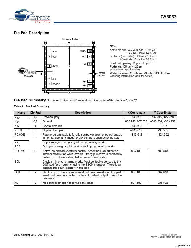
Note Active die size: X = 75.0 mils / 1907 μm Y = 56.2 mils / 1428 μm Scribe: Y (horizontal) = 2.8 mils / 71 μm X (vertical) = 3.4 mils / 86.2 μm Bond pad opening: 85 μm x 85 μm Pad pitch: 125 μm x 125 μm (pad center to pad center) Wafer thickness: 11 mils and 29 mils TYPICAL (See Ordering Information table for details) Die Pad Summary [Pad coordinates are referenced from the center of the die (X = 0, Y = 0)] Table 1. Die Pad Summary Name VDD VSS XIN XOUT PD#/OE VPP SDA SSON# 10 Die Pad 1,2 6,
📁 CY5057 Similar Datasheet