FDD86110
Features
General Description
- Shielded Gate MOSFET Technology
- Max r DS(on) = 10.2 mΩ at VGS = 10 V, ID = 12.5 A
- Max r DS(on) = 16 mΩ at VGS = 6 V, ID = 9.8 A
- 100% UIL tested
This N-Channel MOSFET is produced using Fairchild Semiconductor‘s advanced Power Trench® process that incorporates Shielded Gate technology. This process has been optimized for the on-state resistance and yet maintain superior switching performance.
- Ro HS pliant
Application
- DC
- DC Conversion
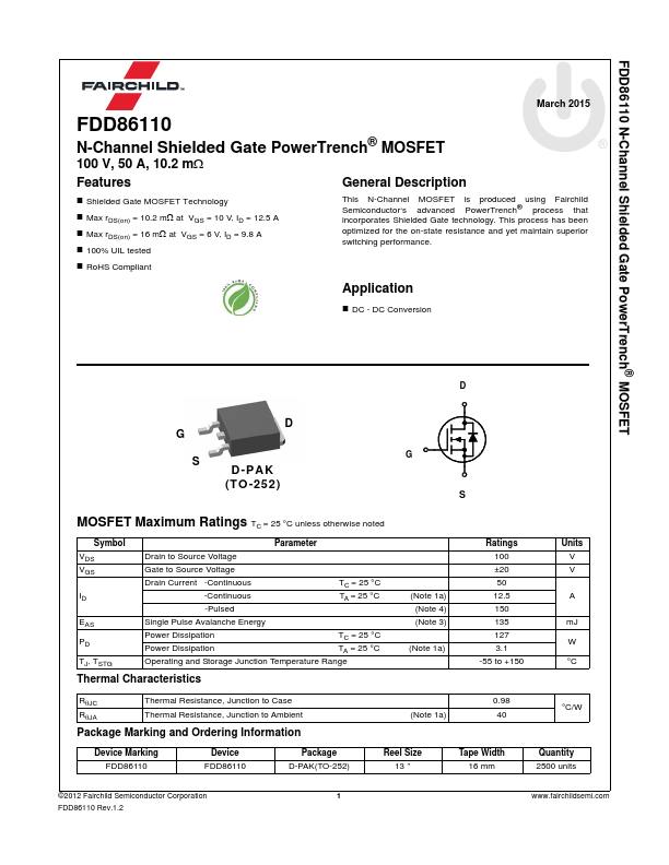
DT O-P-2A5K2 (T O -25 2)
MOSFET Maximum Ratings TC = 25 °C unless otherwise noted
Symbol VDS VGS
EAS PD TJ, TSTG
Parameter
Drain to Source Voltage
Gate to Source Voltage
Drain Current -Continuous -Continuous -Pulsed
TC = 25 °C TA = 25 °C
Single Pulse Avalanche Energy
Power Dissipation
TC = 25 °C
Power Dissipation
TA = 25 °C
Operating and Storage Junction Temperature Range
Thermal Characteristics
(Note 1a) (Note 4) (Note 3)
(Note 1a)
Ratings 100 ±20 50 12.5 150 135 127 3.1
-55 to...