FDD86540 Overview
Key Specifications
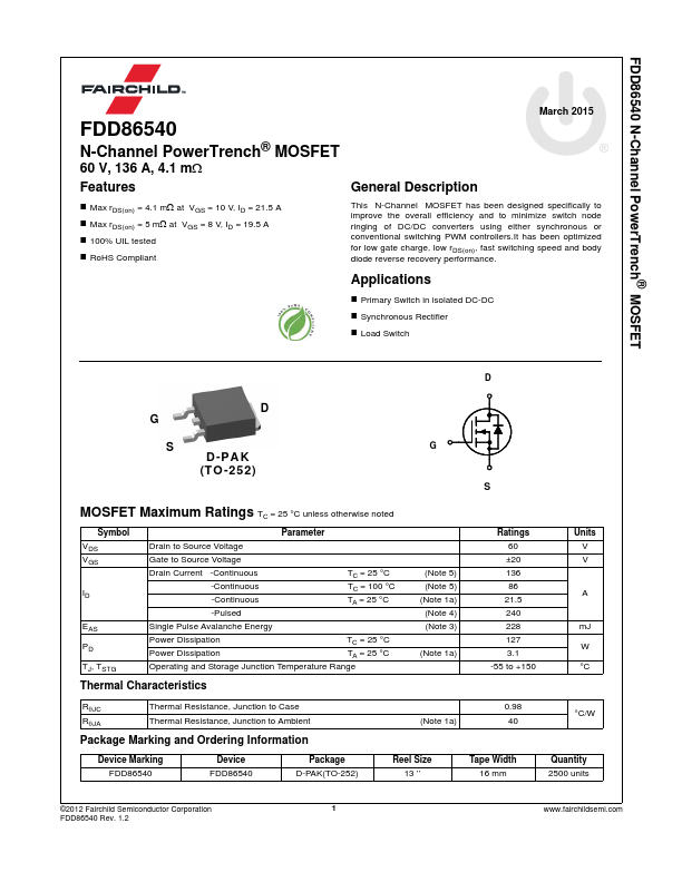
Package: DPAK
Mount Type: Surface Mount
Pins: 3
Height: 2.517 mm
Description
Max rDS(on) = 4.1 mΩ at VGS = 10 V, ID = 21.5 A - Max rDS(on) = 5 mΩ at VGS = 8 V, ID = 19.5 A - 100% UIL tested - RoHS Compliant This N-Channel MOSFET has been designed specifically to improve the overall efficiency and to minimize switch node ringing of DC/DC converters using either synchronous or conventional switching PWM has been optimized for low gate charge, low rDS(on), fast switching speed and body diode reverse recovery performance.