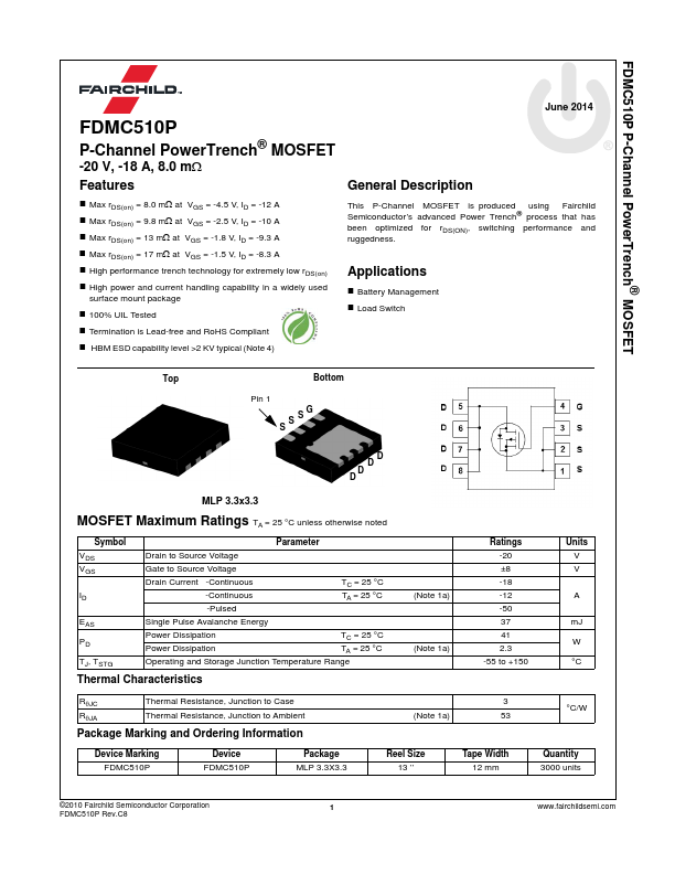
Datasheet4U Logo Datasheet4U.com

FDMC510P - MOSFET

Description

This P-Channel MOSFET is produced using Fairchild Semiconductor’s advanced Power Trench® process that has been optimized for rDS(ON), switching performance and ruggedness.

Battery Management Load Switch Top Bottom Pin 1 S SG S DD D D MLP 3.3x3.3 MOSFET Maximum

Features

  • Max rDS(on) = 8.0 mΩ at VGS = -4.5 V, ID = -12 A.
  • Max rDS(on) = 9.8 mΩ at VGS = -2.5 V, ID = -10 A.
  • Max rDS(on) = 13 mΩ at VGS = -1.8 V, ID = -9.3 A.
  • Max rDS(on) = 17 mΩ at VGS = -1.5 V, ID = -8.3 A.
  • High performance trench technology for extremely low rDS(on).
  • High power and current handling capability in a widely used surface mount package.
  • 100% UIL Tested.
  • Termination is Lead-free and RoHS Compliant.
  • HBM ESD cap.

📥 Download Datasheet

Full PDF Text Transcription (Reference)

The following content is an automatically extracted verbatim text from the original manufacturer datasheet and is provided for reference purposes only.

View original datasheet text
FDMC510P P-Channel PowerTrench® MOSFET FDMC510P P-Channel PowerTrench® MOSFET -20 V, -18 A, 8.0 mΩ Features „ Max rDS(on) = 8.0 mΩ at VGS = -4.5 V, ID = -12 A „ Max rDS(on) = 9.8 mΩ at VGS = -2.5 V, ID = -10 A „ Max rDS(on) = 13 mΩ at VGS = -1.8 V, ID = -9.3 A „ Max rDS(on) = 17 mΩ at VGS = -1.5 V, ID = -8.3 A „ High performance trench technology for extremely low rDS(on) „ High power and current handling capability in a widely used surface mount package „ 100% UIL Tested „ Termination is Lead-free and RoHS Compliant „ HBM ESD capability level >2 KV typical (Note 4) June 2014 General Description This P-Channel MOSFET is produced using Fairchild Semiconductor’s advanced Power Trench® process that has been optimized for rDS(ON), switching performance and ruggedness.
Published: |