FDY4001CZ
Features
Q1: N-Channel
- Max r DS(on) = 5Ω at VGS = 4.5V, ID = 200m A
- Max r DS(on) = 7Ω at VGS = 2.5V, ID = 175m A
- Max r DS(on) = 9Ω at VGS = 1.8V, ID = 150m A Q2: P-Channel tm
General Description
This plementary N & P-Channel MOSFET has been designed using Fairchild Semiconductor’s advanced Power Trench® process to optimize the r DS(ON) @ VGS=2.5V and specify the r DS(ON) @ VGS = 1.8V.
Applications
- Level shifting
- Power Supply Converter Circuits
- Load/Power Switching Cell Phones, Pagers
- Max r DS(on) = 8Ω at VGS = -4.5V, ID = -150m A
- Max r DS(on) = 12Ω at VGS = -2.5V, ID = -125m A
- Max r DS(on) = 15Ω at VGS = -1.8V, ID = -100m A
- ESD protection diode (note 3)
- Ro HS pliant
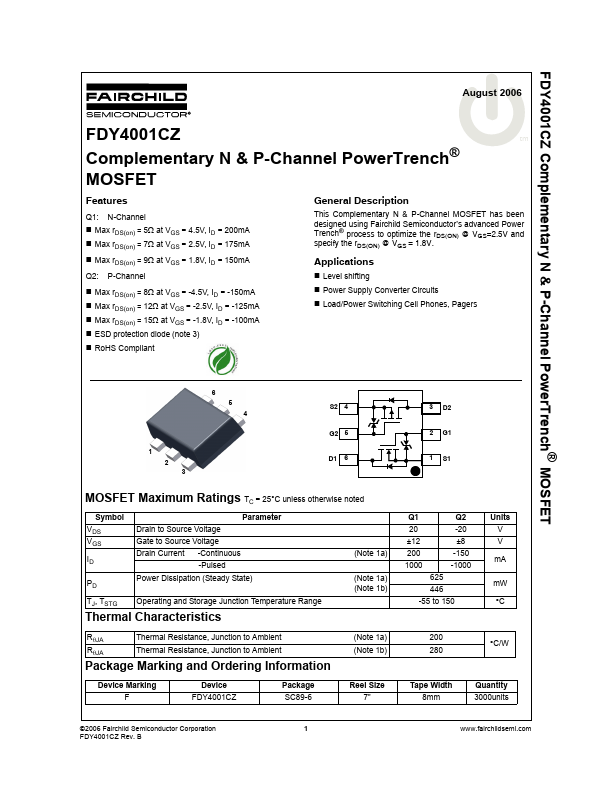
6 5 4
..
S2 4
D2
G2 5
G1
1 2 3
D1
S1
MOSFET Maximum Ratings TC = 25°C unless otherwise noted
Symbol VDS VGS ID PD TJ, TSTG Parameter Drain to Source Voltage Gate to Source Voltage Drain Current -Continuous -Pulsed Power Dissipation (Steady State) Operating and Storage Junction Temperature...