FDY4000CZ
FDY4000CZ is Complementary N & P-Channel PowerTrench MOSFET manufactured by Fairchild Semiconductor.
Features
Q1: N-Channel
- Max r DS(on) = 0.7Ω at VGS = 4.5V, ID = 600m A
- Max r DS(on) = 0.85Ω at VGS = 2.5V, ID = 500m A
- Max r DS(on) = 1.25Ω at VGS = 1.8V, ID =150 m A Q2: P-Channel
- Level shifting
- Power Supply Converter Circuits
- Load/Power Switching Cell Phones, Pagers tm
General Description
This plementary N & P-Channel MOSFET has been designed using Fairchild Semiconductor’s advanced Power Trench® process to optimize the r DS(ON) @ VGS= 2.5V and specify the r DS(ON) @ VGS = 1.8V.
Applications
- Max r DS(on) = 1.2Ω at VGS = -4.5V, ID = -350m A
- Max r DS(on) = 1.6Ω at VGS = -2.5V, ID = -300m A
- Max r DS(on) = 2.7Ω at VGS = -1.8V, ID = -150m A
- ESD protection diode (note 3)
- Ro HS pliant
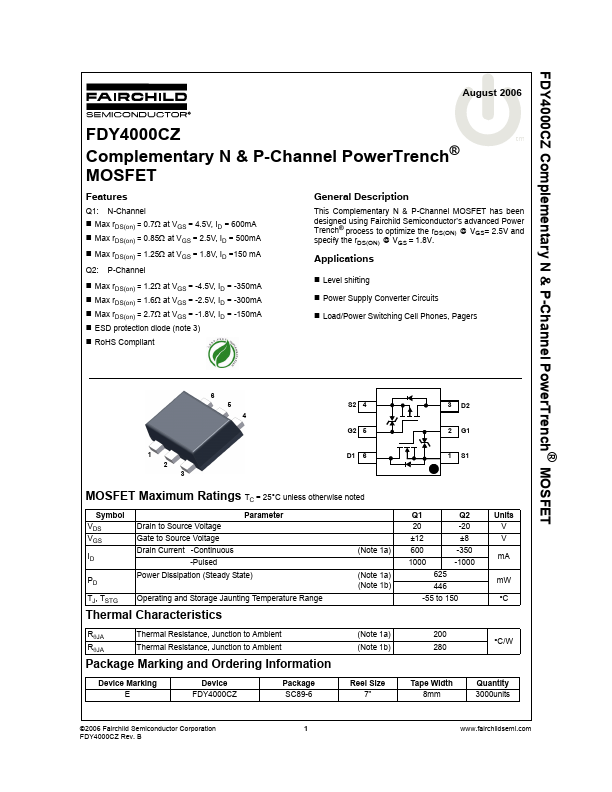
6 5 4
..
S2 4
D2
G2 5
G1
1 2 3
D1
S1
MOSFET Maximum Ratings TC = 25°C unless otherwise noted
Symbol VDS VGS ID PD TJ, TSTG Parameter Drain to Source Voltage Gate to Source Voltage Drain Current -Continuous -Pulsed Power Dissipation (Steady State) Operating and Storage Jaunting Temperature Range (Note 1a) (Note 1b) (Note 1a) Q1 20 ±12 600 1000 625 446 -55 to 150 Q2 -20 ±8 -350 -1000 Units V V m A m W °C
Thermal Characteristics
RθJA RθJA Thermal Resistance, Junction to Ambient Thermal Resistance, Junction to Ambient (Note 1a) (Note 1b) 200 280 °C/W
Package Marking and Ordering Information
Device Marking E Device FDY4000CZ Package SC89-6 Reel Size 7” Tape Width 8mm Quantity 3000units
©2006 Fairchild Semiconductor Corporation FDY4000CZ Rev. B
.fairchildsemi.
FDY4000CZ plementary N & P-Channel Power Trench® MOSFET
Electrical Characteristics TJ = 25°C unless otherwise...