The following content is an automatically extracted verbatim text
from the original manufacturer datasheet and is provided for reference purposes only.
View original datasheet text
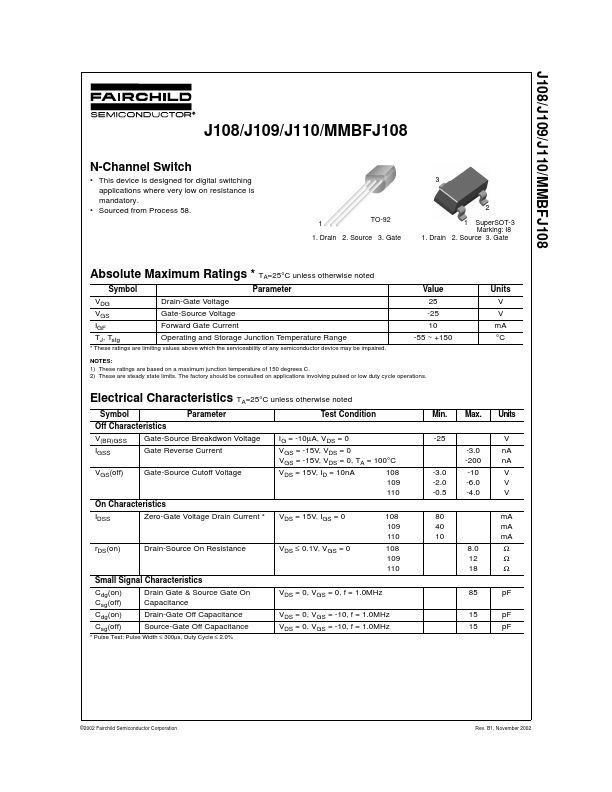
J108/J109/J110/MMBFJ108
J108/J109/J110/MMBFJ108
N-Channel Switch
• This device is designed for digital switching applications where very low on resistance is mandatory.
• Sourced from Process 58.
3
1 TO-92 1. Drain 2. Source 3. Gate
2
1 SuperSOT-3 Marking: I8
1. Drain 2. Source 3. Gate
Absolute Maximum Ratings * TA=25°C unless otherwise noted
Symbol
Parameter
VDG Drain-Gate Voltage
VGS Gate-Source Voltage
IGF Forward Gate Current
TJ, Tstg
Operating and Storage Junction Temperature Range
* These ratings are limiting values above which the serviceability of any semiconductor device may be impaired.
Value 25 -25 10
-55 ~ +150
NOTES: 1) These ratings are based on a maximum junction temperature of 150 degrees C. 2) These are steady state limits.
 J108 Datasheet