Datasheet Details
| Part number | 33389 |
|---|---|
| Manufacturer | Freescale Semiconductor |
| File Size | 761.53 KB |
| Description | System Basis Chip |
| Datasheet |
 33389_FreescaleSemiconductor.pdf 33389_FreescaleSemiconductor.pdf
|
| Part number | 33389 |
|---|---|
| Manufacturer | Freescale Semiconductor |
| File Size | 761.53 KB |
| Description | System Basis Chip |
| Datasheet |
33389_FreescaleSemiconductor.pdf
|
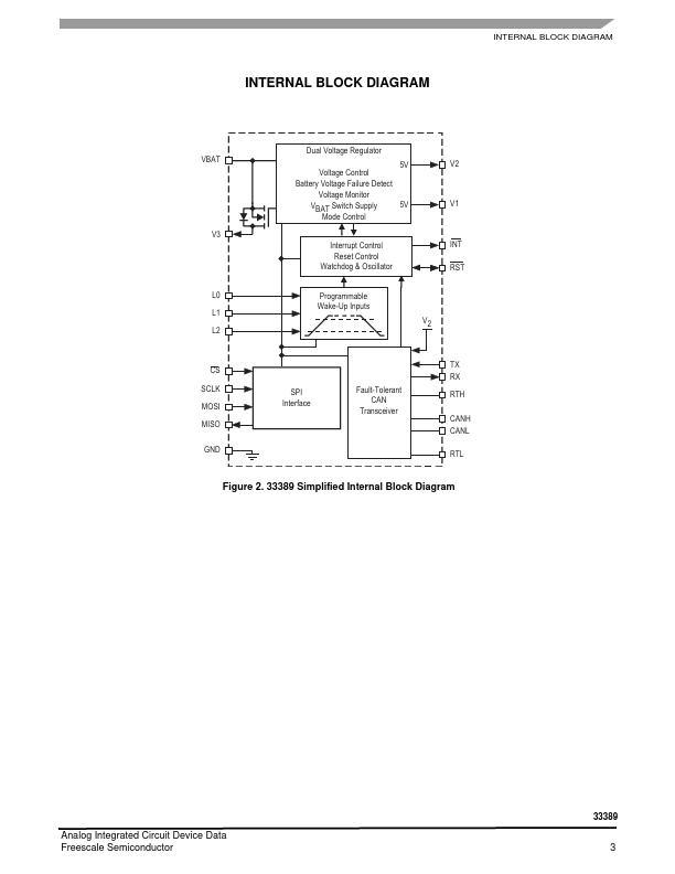
of each pin can be found in the Functional Pin Description section beginning on page 17.
📁 33389 Similar Datasheet