Description
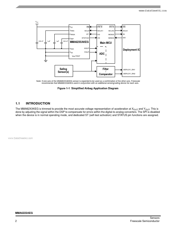
VCC
This pin supplies power to the device.Careful printed wiring board layout and capacitor placement is critical to ensure best performance.An external bypass capacitor between this pin and VSS is required, as described in Section 1.5.
1.4.2
VSS VSSA
This pin is the power supply return node for the digital circuitry on the MMA62XXKEG device.1.4.3
This pin is the power supply return node for analog circuitry on the MMA62XXAKEG device.An external bypass capacitor between this pin and V
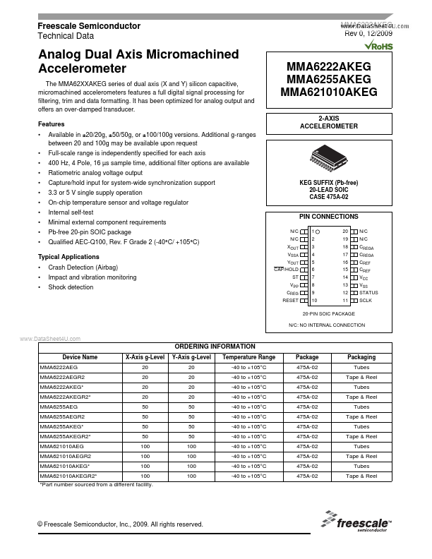
Features
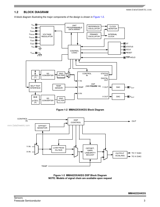
- a full digital signal processing for filtering, trim and data formatting. It has been optimized for analog output and offers an over-damped transducer. Features.
- Available in ±20/20g, ±50/50g, or ±100/100g versions. Additional g-ranges between 20 and 100g may be available upon request Full-scale range is independently specified for each axis 400 Hz, 4 Pole, 16 µs sample time, additional f.
 MMA6222AEG_FreescaleSemiconductor.pdf