Description
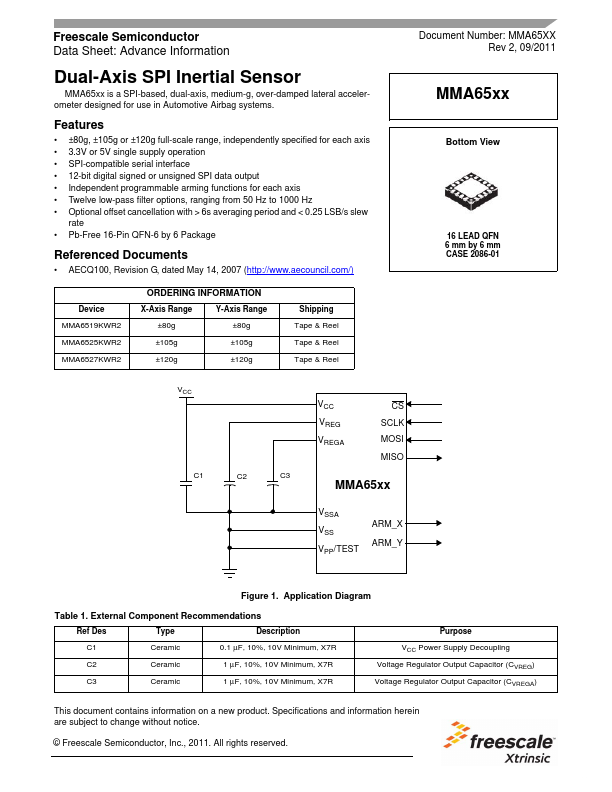
0.1 μF, 10%, 10V Minimum, X7R 1 μF, 10%, 10V Minimum, X7R 1 μF, 10%, 10V Minimum, X7R Purpose VCC Power Supply Decoupling Voltage Regulator Output Capacitor (CVREG) Voltage Regulator Output Capacitor (CVREGA)
This document contains information on a new product.Specifications and information herein are subject to change without notice.© Freescale Semiconductor, Inc., 2011. All rights reserved.Datasheet pdf - http://www.DataSheet4U.net/
www.DataSheet.co.kr
VCC VREG VREGA VSS
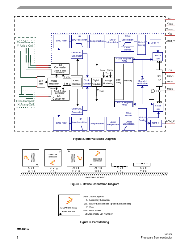
IIR Offset Comp
Features
- ±80g, ±105g or ±120g full-scale range, independently specified for each axis 3.3V or 5V single supply operation SPI-compatible serial interface 12-bit digital signed or unsigned SPI data output Independent programmable arming functions for each axis Twelve low-pass filter options, ranging from 50 Hz to 1000 Hz Optional offset cancellation with > 6s averaging period and < 0.25 LSB/s slew rate Pb-Free 16-Pin QFN-6 by 6.
 MMA65xx_MotorolaSemiconductorProducts.pdf