Description
Table
Symbol
Description
Type Comments
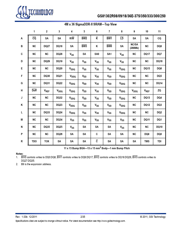
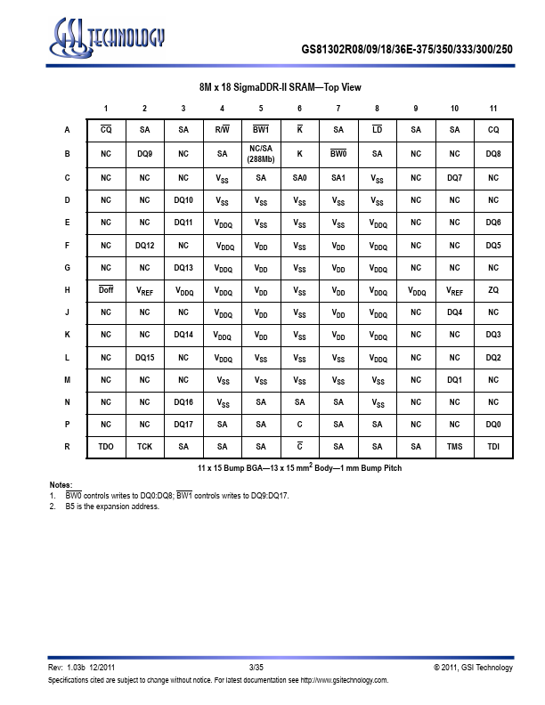
SA
Synchronous Address Inputs
Input
R/W
Synchronous Read/Write
Input
Read: Active High Write: Active Low
BW0
BW3
Synchronous Byte Writes
Input
Active Low x18/x36 only
NW0
NW1
Nybble Write Control Pin
Input
Active Low x8 only
LD
Synchronous Load Pin
Input Active Low
K
Input Clock
Input Active High
K
Input Clock
Input Active Low
C
Output Clock
Input Active High
C
Output Clock
Input Active Low
TMS
Te
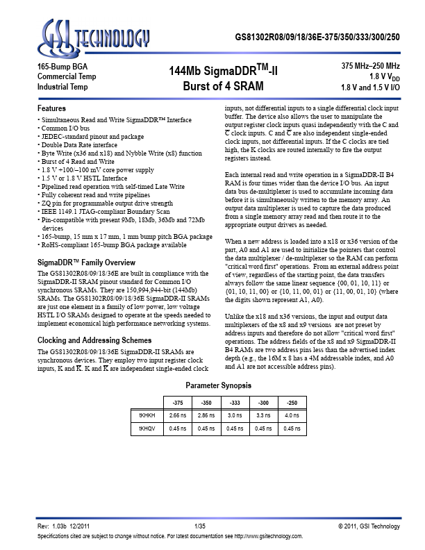
Features
- Simultaneous Read and Write SigmaDDR™ Interface.
- Common I/O bus.
- JEDEC-standard pinout and package.
- Double Data Rate interface.
- Byte Write (x36 and x18) and Nybble Write (x8) function.
- Burst of 4 Read and Write.
- 1.8 V +100/.
- 100 mV core power supply.
- 1.5 V or 1.8 V HSTL Interface.
- Pipelined read operation with self-timed Late Write.
- Fully coherent read and write pipelines.
- ZQ pin for progra.


