Description
Table
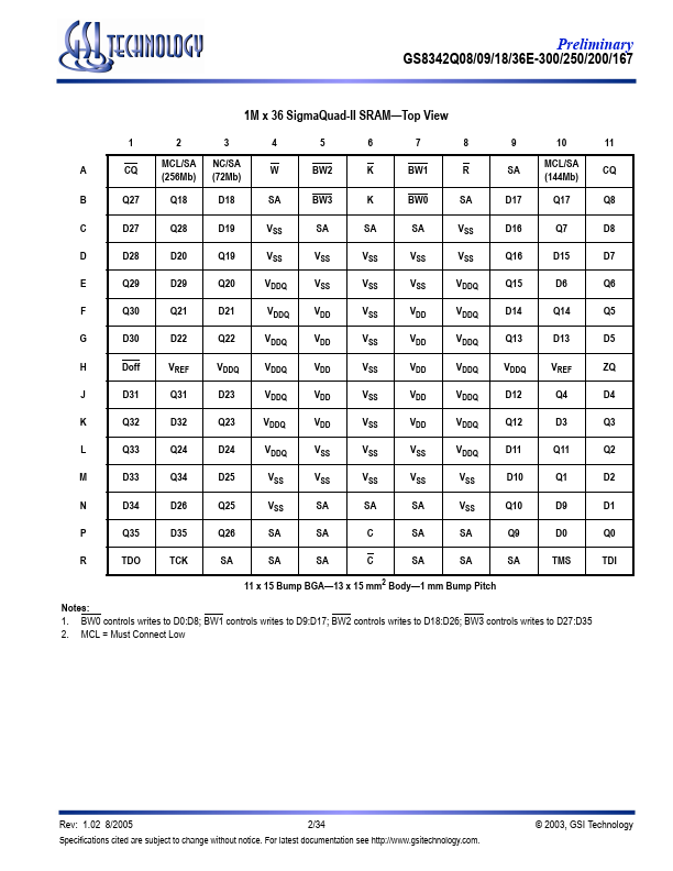
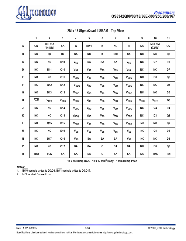
Symbol
SA NC R W
BW
Description
Synchronous Address Inputs No Connect
Synchronous Read Synchronous Write
Synchronous Byte Write
BW0
BW3
Synchronous Byte Writes
NW0
NW1
Nybble Write Control Pin
K Input Clock
K Input Clock
C Output Clock
C Output Clock
TMS Test Mode Select
TDI Test Data Input
TCK Test Clock Input
TDO Test Data Output
VREF HSTL Input Reference Voltage
ZQ Output Impedance Matching Input
Qn Synchronous Data Outputs
Dn Synchronous Data Inputs
Do
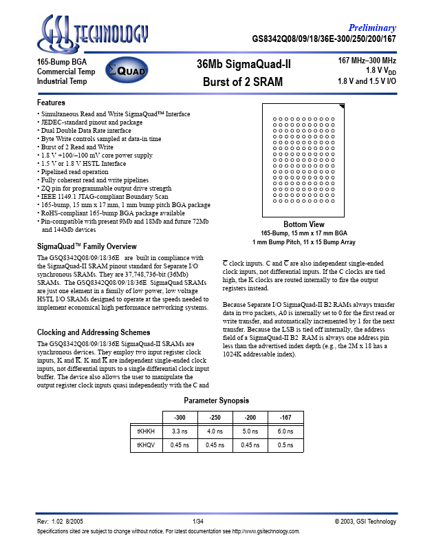
Features
- Simultaneous Read and Write SigmaQuad™ Interface.
- JEDEC-standard pinout and package.
- Dual Double Data Rate interface.
- Byte Write controls sampled at data-in time.
- Burst of 2 Read and Write.
- 1.8 V +100/.
- 100 mV core power supply.
- 1.5 V or 1.8 V HSTL Interface.
- Pipelined read operation.
- Fully coherent read and write pipelines.
- ZQ pin for programmable output drive strength.
- IEEE 1149.1 JTAG-co.
 GS8342Q08E-300-GSITechnology.pdf