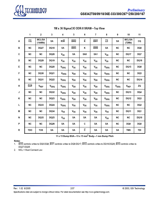
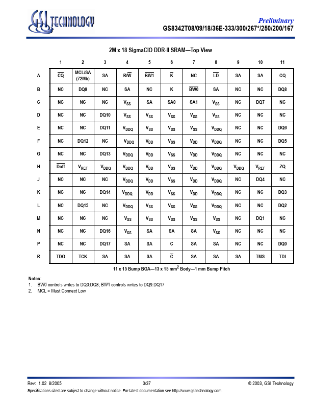
Description
Table Symbol
SA NC R/W BW0
BW3 NW0
NW1 LD K K C C TMS TDI TCK TDO VREF ZQ DQ Doff CQ CQ VDD VDDQ VSS Note: NC = Not Connected to die or any other pin
Description
Synchronous Address Inputs No Connect Synchronous Read/Write Synchronous Byte Writes Nybble Write Control Pin Synchronous Load Pin Input Clock Input Clock Output Clock Output Clock Test Mode Select Test Data Input Test Clock Input Test Data Output HSTL Input Reference Voltage
http://www.DataSheet4U.net/
Type
Input
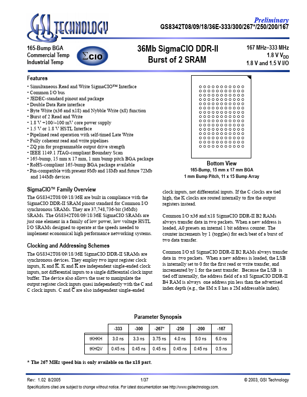
Features
- Simultaneous Read and Write SigmaCIO™ Interface.
- Common I/O bus.
- JEDEC-standard pinout and package.
- Double Data Rate interface.
- Byte Write (x36 and x18) and Nybble Write (x8) function.
- Burst of 2 Read and Write.
- 1.8 V +100/.
- 100 mV core power supply.
- 1.5 V or 1.8 V HSTL Interface.
- Pipelined read operation with self-timed Late Write.
- Fully coherent read and write pipelines.
- ZQ pin for progra.
 GS8342T36E-250 Datasheet