Datasheet4U Logo Datasheet4U.com

GS88019AT - 9Mb Sync Burst SRAMs

Datasheet Summary

Description

Pin Location 37, 36 35, 34, 33, 32, 100, 99, 82, 81, 44, 45, 46, 47, 48, 49, 50, 43 80 63, 62, 59, 58, 57, 56, 53, 52 68, 69, 72, 73, 74, 75, 78, 79 13, 12, 9, 8, 7, 6, 3, 2 18, 19, 22, 23, 24, 25, 28, 29 51, 80, 1, 30 14, 16, 38, 39, 42, 66 51, 80, 1, 30 58, 59, 62, 63, 68, 69, 72, 73, 74 8, 9, 12,

Features

  • Single Cycle Deselect (SCD) operation.
  • 2.5 V or 3.3 V +10%/.
  • 10% core power supply.
  • 2.5 V or 3.3 V I/O supply.
  • LBO pin for Linear or Interleaved Burst mode.
  • Internal input resistors on mode pins allow floating mode pins.
  • Default to Interleaved Pipeline mode.
  • Byte Write (BW) and/or Global Write (GW) operation.
  • Internal self-timed write cycle.
  • Automatic power-down for portable.

📥 Download Datasheet

Datasheet preview – GS88019AT

Datasheet Details

Part number GS88019AT
Manufacturer GSI Technology
File Size 748.17 KB
Description 9Mb Sync Burst SRAMs
Datasheet download datasheet GS88019AT Datasheet
Additional preview pages of the GS88019AT datasheet.
Other Datasheets by GSI Technology

Full PDF Text Transcription

Click to expand full text
Datasheet Errata Revision: 5/17/02 GS88019/33/37AT Base datasheet: GS88019/33/37AT, Rev.1.00, 3/2002 Product(s) covered in this supplement: GS88019/33/37AT-250/225/200/166/150/133 Product specification(s) addressed by this supplement:
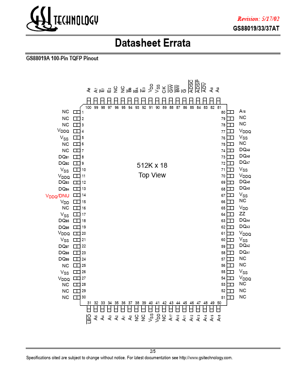
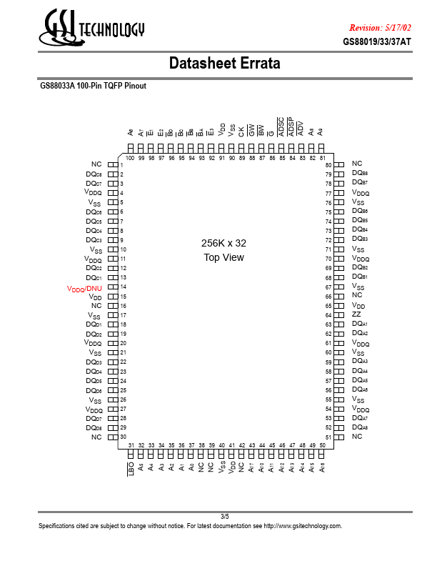
 Pin 14 Note: The specifications cited in the base datasheet for the products addressed by this errata remain in force except where superseded by the information in this errata. 1/5 Specifications cited are subject to change without notice. For latest documentation see http://www.gsitechnology.com.
Published: |