9LPRS365 Overview
Key Specifications
Package: TSSOP
Mount Type: Surface Mount
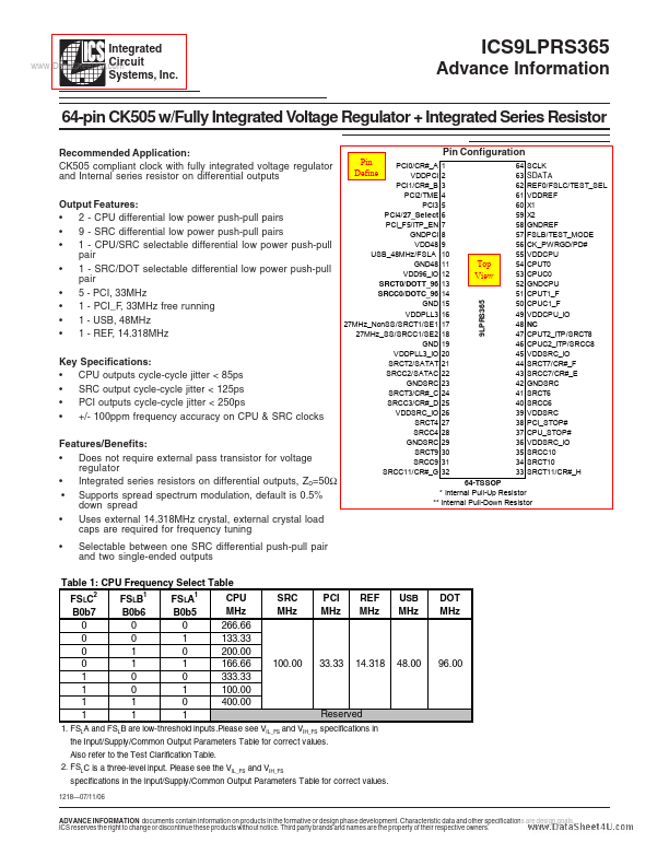
Pins: 64
Operating Voltage: 3.3 V
Key Features
- 2 - CPU differential low power push-pull pairs
- 9 - SRC differential low power push-pull pairs
- 1 - CPU/SRC selectable differential low power push-pull pair
- 1 - SRC/DOT selectable differential low power push-pull pair
- 5 - PCI, 33MHz