IN74HC00A
TECHNICAL DATA
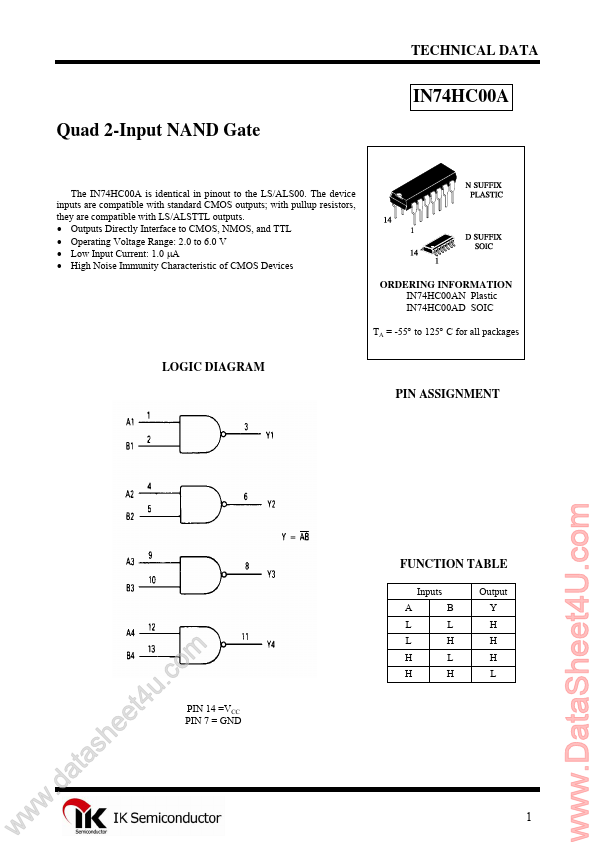
IN74HC00A Quad 2-Input NAND Gate
The IN74HC00A is identical in pinout to the LS/ALS00. The device inputs are patible with standard CMOS outputs; with pullup resistors, they are patible with LS/ALSTTL outputs.
- Outputs Directly Interface to CMOS, NMOS, and TTL
- Operating Voltage Range: 2.0 to 6.0 V
- Low Input Current: 1.0 µA
- High Noise Immunity Characteristic of CMOS Devices ORDERING INFORMATION IN74HC00AN Plastic IN74HC00AD SOIC TA = -55° to 125° C for all packages
LOGIC DIAGRAM PIN ASSIGNMENT
FUNCTION TABLE
Inputs A L L H H B L H L H Output Y H H H L w w w
.d h s a t a ee
. u t4 m o c
PIN 14 =VCC PIN 7 = GND
..
MAXIMUM RATINGS-
Symbol VCC VIN VOUT IIN IOUT ICC PD Tstg TL
- Parameter DC Supply Voltage (Referenced to GND) DC Input Voltage (Referenced to GND) DC Output Voltage (Referenced to GND) DC Input Current, per Pin DC Output Current, per Pin DC Supply Current, VCC and GND Pins Power Dissipation in Still Air, Plastic DIP SOIC...