IW4011B
TECHNICAL DATA
Quad 2-Input NAND Gate
High-Voltage Silicon-Gate CMOS
The IW4011B NAND gates provide the system designer with direct emplementation of the NAND function.
- Operating Voltage Range: 3.0 to 18 V
- Maximum input current of 1 µA at 18 V over full package-temperature range; 100 n A at 18 V and 25°C
- Noise margin (over full package temperature range): 1.0 V min @ 5.0 V supply 2.0 V min @ 10.0 V supply 2.5 V min @ 15.0 V supply
ORDERING INFORMATION IW4011BN Plastic IW4011BD SOIC TA = -55° to 125° C for all packages
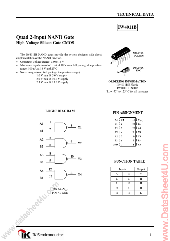
LOGIC DIAGRAM
PIN ASSIGNMENT
FUNCTION TABLE
Inputs A L L H H B L H L H Output Y H H H L w w w
.d e e h s a t a
. u t4 m o c
PIN 14 =VCC PIN 7 = GND
..
MAXIMUM RATINGS-
Symbol VCC VIN VOUT IIN PD PD Tstg TL
- Parameter DC Supply Voltage (Referenced to GND) DC Input Voltage (Referenced to GND) DC Output Voltage (Referenced to GND) DC Input Current, per Pin Power Dissipation in Still Air, Plastic DIP+ SOIC Package+ Power Dissipation...