Datasheet4U Logo Datasheet4U.com

IS43TR16256B - 4Gb DDR3 SDRAM

Download the IS43TR16256B datasheet PDF. This datasheet also covers the IS46TR16256B variant, as both devices belong to the same 4gb ddr3 sdram family and are provided as variant models within a single manufacturer datasheet.

Description

- JEDEC Standard Sy

Features

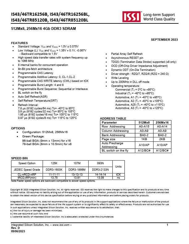
  • Standard Voltage: VDD and VDDQ = 1.5V ± 0.075V.
  • Low Voltage (L): VDD and VDDQ = 1.35V + 0.1V, -0.067V - Backward compatible to 1.5V.
  • High speed data transfer rates with system frequency up to 1066 MHz.
  • 8 internal banks for concurrent operation.
  • 8n-Bit pre-fetch architecture.
  • Programmable CAS Latency.
  • Programmable Additive Latency: 0, CL-1,CL-2.
  • Programmable CAS WRITE latency (CWL) based on tCK.
  • Programmable Burst L.

📥 Download Datasheet

Note: The manufacturer provides a single datasheet file (IS46TR16256B-ISSI.pdf) that lists specifications for multiple related part numbers.

Full PDF Text Transcription (Reference)

The following content is an automatically extracted verbatim text from the original manufacturer datasheet and is provided for reference purposes only.

View original datasheet text
IS43/46TR16256B, IS43/46TR16256BL, IS43/46TR85120B, IS43/46TR85120BL 512Mx8, 256Mx16 4Gb DDR3 SDRAM FEATURES • Standard Voltage: VDD and VDDQ = 1.5V ± 0.075V • Low Voltage (L): VDD and VDDQ = 1.35V + 0.1V, -0.067V - Backward compatible to 1.5V • High speed data transfer rates with system frequency up to 1066 MHz • 8 internal banks for concurrent operation • 8n-Bit pre-fetch architecture • Programmable CAS Latency • Programmable Additive Latency: 0, CL-1,CL-2 • Programmable CAS WRITE latency (CWL) based on tCK • Programmable Burst Length: 4 and 8 • Programmable Burst Sequence: Sequential or Interleave • BL switch on the fly • Auto Self Refresh(ASR) • Self Refresh Temperature(SRT) • Refresh Interval: 7.8 µs (8192 cycles/64 ms) Tc= -40°C to 85°C 3.
Published: |