Datasheet Details
- Part number
- HYS64V64220GBDL-8-D
- Manufacturer
- Infineon ↗
- File Size
- 456.00 KB
- Datasheet
-
 HYS64V64220GBDL-8-D_InfineonTechnologiesAG.pdf
- Description
- 144 pin SO-DIMM SDRAM Modules
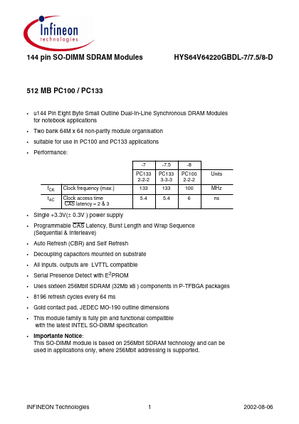
 HYS64V64220GBDL-8-D_InfineonTechnologiesAG.pdf
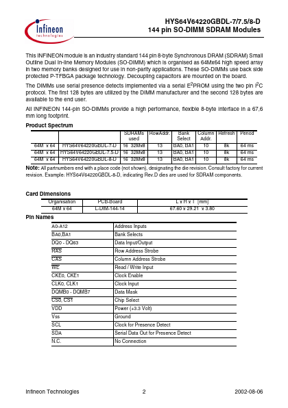
in this drawing, however DQ/DQMB/CKE/CS relationship is maintained as shown.
📁 Similar Datasheet