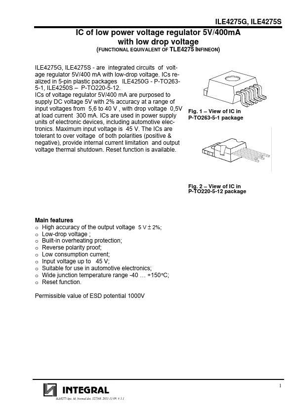
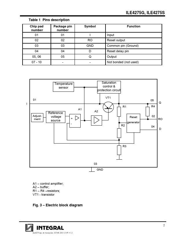
Description
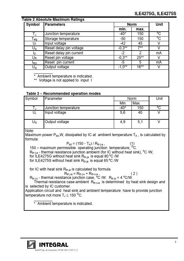
Chip pad number
01 02 03 04 05, 06 07 - 10
Package pin number 01 02 03 04 05 -
ILE4275G, ILE4275S
Symbol
I RO GND D Q
-
Function
Input Reset output Common pin (Ground) Reset delay pin Output Not bonded (not used)
Temperature sensor
01 I
Adjustment
Reference voltage source
A1
+ -
Saturation control & protection circuit
VT1
R1 A2
Reset generator R2
05 Q
R4
02 RO
04 D
R3
03 GND
A1
control amplifier; A2
buffer; R1
R4
resistors; VT1 - transistor
Fi
Features
- o High accuracy of the output voltage 5 V ± 2%; o Low-drop voltage ; o Built-in overheating protection; o Reverse polarity proof; o Low consumption current; o Input voltage up to 45 V; o Suitable for use in automotive electronics; o Wide junction temperature range -40 … +150°C; o Reset function. Permissible value of ESD potential 1000V
ILE4275-Spe, M, Normal. dot, 327168, 2011-11-09, V 1.1
1
Table 1 Pins.
 ILE4275G-Integral.pdf