Datasheet Details
- Part number
- ICS508
- Manufacturer
- Integrated Circuit Systems
- File Size
- 49.16 KB
- Datasheet
- ICS508_IntegratedCircuitSystems.pdf
- Description
- PECL to CMOS Converter
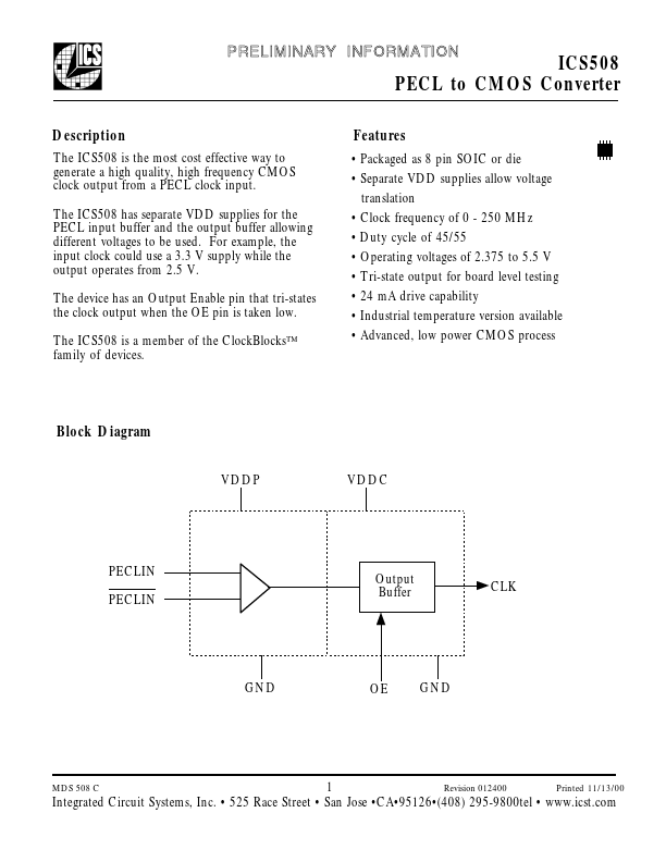
ICS508 Description
PRELIMINARY INFORMATION ICS508 PECL to CMOS Converter .
The ICS508 is the most cost effective way to generate a high quality, high frequency CMOS clock output from a PECL clock input.
ICS508 Features
* Packaged as 8 pin SOIC or die
* Separate VDD supplies allow voltage translation
* Clock frequency of 0 - 250 MHz
* Duty cycle of 45/55
* Operating voltages of 2.375 to 5.5 V
* Tri-state output for board level testing
* 24 mA drive capability
ICS508 Applications
* Any other applications such as those requiring extended temperature range, high reliability, or other extraordinary environmental requirements are not recommended without additional processing by ICS. ICS reserves the right to change any circuitry or specifications without notice. ICS does not auth
📁 Related Datasheet
📌 All Tags