Datasheet4U Logo Datasheet4U.com

CD40175BMS - CMOS Quad D Type Flip-Flop

General Description

of ‘B’ Series CMOS Devices” Q1 2 Q1 3 D1 4 D2 5 Q2 6 Q2 7 VSS 8 VDD = PIN 16 VSS = PIN 8 Functional Diagram 4 F/F1 2 3 Applications Shift Registers Buffer/Storage Registers Pattern Generators D2 D1 Q1 Q1 5 F/F2 7 6 Q2 Q2 Description CD40175BMS consists of four i

Key Features

  • High Voltage Type (20V Rating).
  • Output Compatible with Two HTL Loads, Two Low Power TTL Loads, or One Low Power Schottky TTL Load CLEAR 1 16 VDD 15 Q4 14 Q4 13 D4 12 D3 11 Q3 10 Q3 9 CLOCK.
  • Functional Equivalent to TTL74175.
  • 100% Tested for Quiescent Current at 20V.
  • 5V, 10V and 15V Parametric Ratings.
  • Maximum Input Current of 1µA at 18V Over Full Package Temperature Range; 100nA at 18V and +25oC.
  • Noise Margin (Over Full Package/T.

📥 Download Datasheet

Full PDF Text Transcription (Reference)

The following content is an automatically extracted verbatim text from the original manufacturer datasheet and is provided for reference purposes only.

View original datasheet text
CD40175BMS December 1992 CMOS Quad ‘D’ Type Flip-Flop
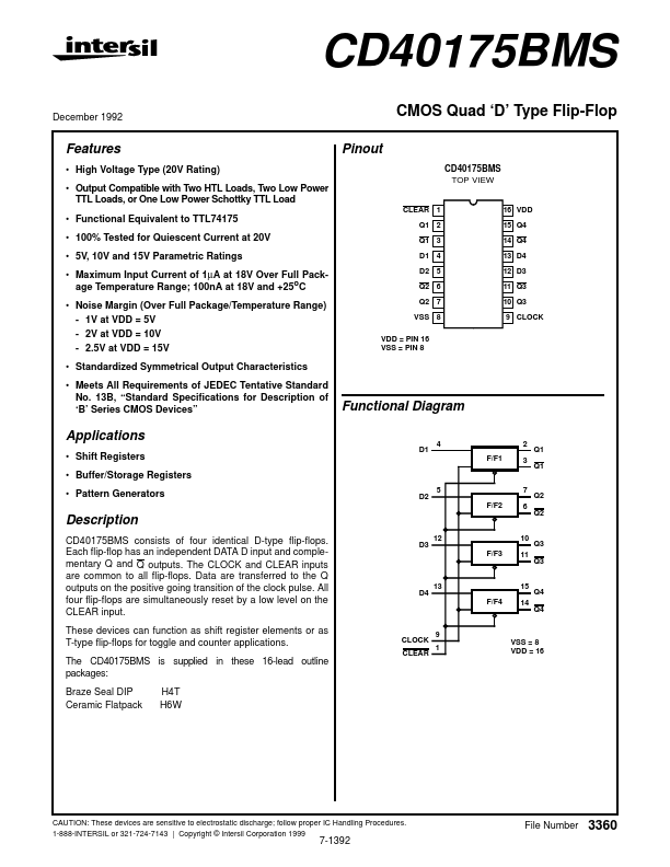
 Pinout CD40175BMS TOP VIEW Features • High Voltage Type (20V Rating) • Output Compatible with Two HTL Loads, Two Low Power TTL Loads, or One Low Power Schottky TTL Load CLEAR 1 16 VDD 15 Q4 14 Q4 13 D4 12 D3 11 Q3 10 Q3 9 CLOCK • Functional Equivalent to TTL74175 • 100% Tested for Quiescent Current at 20V • 5V, 10V and 15V Parametric Ratings • Maximum Input Current of 1µA at 18V Over Full Package Temperature Range; 100nA at 18V and +25oC • Noise Margin (Over Full Package/Temperature Range) - 1V at VDD = 5V - 2V at VDD = 10V - 2.5V at VDD = 15V • Standardized Symmetrical Output Characteristics • Meets All Requirements of JEDEC Tentative Standard No.