CD40175BM Datasheet Text
CD40174BM CD40174BC Hex D Flip-Flop CD40175BM CD40175BC Quad D Flip-Flop
February 1988
CD40174BM CD40174BC Hex D Flip-Flop CD40175BM CD40175BC Quad D Flip-Flop
General Description
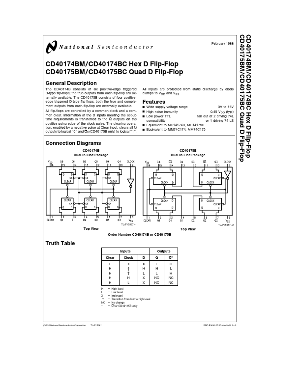
The CD40174B consists of six positive-edge triggered D-type flip-flops the true outputs from each flip-flop are externally available The CD40175B consists of four positiveedge triggered D-type flip-flops both the true and plement outputs from each flip-flop are externally available All flip-flops are controlled by a mon clock and a mon clear Information at the D inputs meeting the set-up time requirements is transferred to the Q outputs on the positive-going edge of the clock pulse The clearing operation enabled by a negative pulse at Clear input clears all Q outputs to logical ‘‘0’’ and Qs (CD40175B only) to logical ‘‘1’’ All inputs are protected from static discharge by diode clamps to VDD and VSS
Features
Y Y Y
Y Y
Wide supply voltage range 3V to 15V High noise immunity 0 45 VDD (typ ) Low power TTL fan out of 2 driving 74L patibility or 1 driving 74 LS Equivalent to MC14174B MC14175B Equivalent to MM74C174 MM74C175
Connection Diagrams
CD40174B Dual-In-Line Package CD40175B Dual-In-Line Package
TL F 5987
- 1
TL F 5987
- 2
Top View Order Number CD40174B or CD40175B
Top View
Truth Table
Inputs Clear L H H H H
H L X NC e e e e e e
Outputs D X H L X X Q L H L NC NC Q H L H NC NC
Clock X u u
H L u
High level Low level Irrelevant Transition from low to high level No change Q for CD40175B only
C1995 National Semiconductor Corporation
TL F 5987
RRD-B30M105 Printed in U S...