CD40174BMS
Description
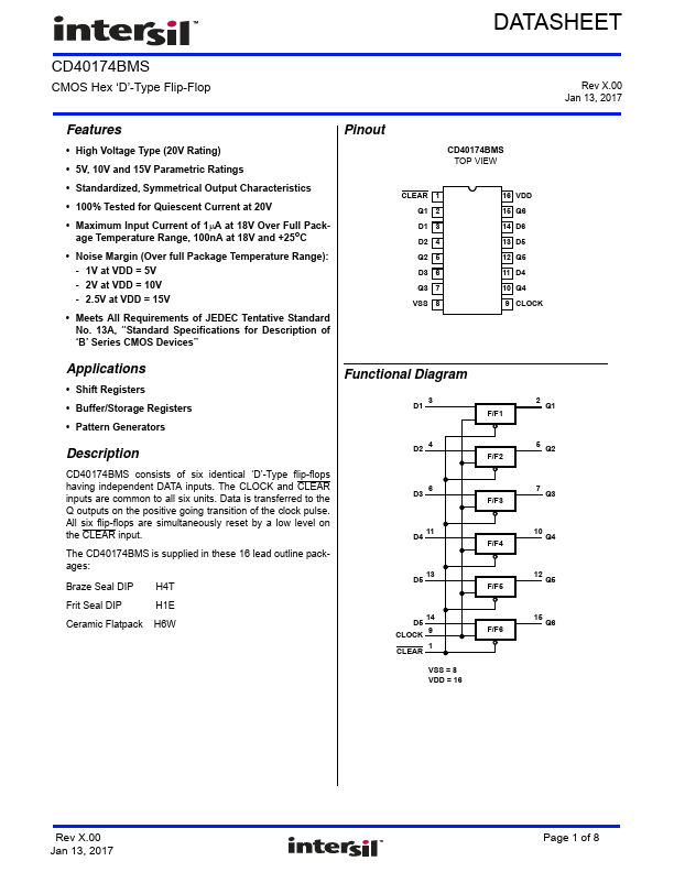
D2 4 CD40174BMS consists of six identical ‘D’-Type flip-flops having independent DATA inputs.
Key Features
- High Voltage Type (20V Rating)
- Standardized, Symmetrical Output Characteristics
- 100% Tested for Quiescent Current at 20V
- Maximum Input Current of 1A at 18V Over Full Package Temperature Range, 100nA at 18V and +25oC
- Noise Margin (Over full Package Temperature Range): - 1V at VDD = 5V - 2V at VDD = 10V - 2.5V at VDD = 15V
- Meets All Requirements of JEDEC Tentative Standard No. 13A, “Standard Specifications for Description of ‘B’ Series CMOS Devices”
Applications
- Shift Registers