CD40175BMS
Description
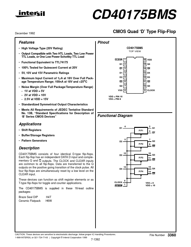
CD40175BMS consists of four identical D-type flip-flops. Each flip-flop has an independent DATA D input and plementary Q and Q outputs.
Key Features
- High Voltage Type (20V Rating)
- Functional Equivalent to TTL74175
- 100% Tested for Quiescent Current at 20V
- 5V, 10V and 15V Parametric Ratings
- Maximum Input Current of 1µA at 18V Over Full Package Temperature Range; 100nA at 18V and +25oC
- Noise Margin (Over Full Package/Temperature Range)
- 1V at VDD = 5V
- 2V at VDD = 10V
- 2.5V at VDD = 15V
- Standardized Symmetrical Output Characteristics