Datasheet Details
| Part number | CD4023BMS |
|---|---|
| Manufacturer | Intersil Corporation |
| File Size | 282.44 KB |
| Description | CMOS NAND Gates |
| Datasheet |
 CD4023BMS_IntersilCorporation.pdf CD4023BMS_IntersilCorporation.pdf
|
|
|
The CD4023BMS by Intersil Corporation is a CMOS NAND Gates. Below is the official datasheet preview.
| Part number | CD4023BMS |
|---|---|
| Manufacturer | Intersil Corporation |
| File Size | 282.44 KB |
| Description | CMOS NAND Gates |
| Datasheet |
CD4023BMS_IntersilCorporation.pdf
|
|
|
|
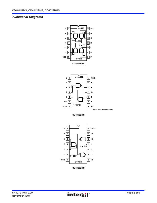
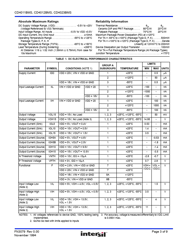
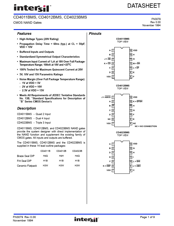
of “B” Series CMOS Device’s J = ABCD 1 A 2 B 3 CD4012BMS TOP VIEW 14 VDD 13 K = EFGH 12 H 11 G 10 F 9 E 8 NC NC = NO CONNECTION Description CD4011BMS - Quad 2 Input CD4012BMS - Dual 4 Input CD4023BMS - Triple 3 Input CD4011BMS, CD4012BMS, and CD4023BMS NAND gates provide the system designer with direct implementation of the NAND function and supplement the existing family of CMOS gates.All inputs and outputs are buffered.The CD4011BMS, CD4012BMS and the CD4023BMS is supplied in these 14 lea
📁 CD4023BMS Similar Datasheet