• Part: CD4099BMS
  • Description: CMOS 8-Bit Addressable Latch
  • Manufacturer: Intersil
  • Size: 110.47 KB
Download CD4099BMS Datasheet PDF
Intersil
CD4099BMS
CD4099BMS is CMOS 8-Bit Addressable Latch manufactured by Intersil.
Features - High Voltage Type (20V Rating) - Serial Data Input - Active Parallel Output Q7 1 2 16 VDD 15 Q6 14 Q5 13 Q4 12 Q3 11 Q2 10 Q1 9 Q0 - Storage Register Capability - Master Clear - Can Function as Demultiplexer - 100% Tested for Quiescent Current at 20V - 5V, 10V and 15V Parametric Ratings - Standardized Symmetrical Output Characteristics - Maximum Input Current of 1µA at 18V Over Full Package Temperature Range; 100n A at 18V and +25o C - Noise Margin (Over Full Package/Temperature Range) - 1V at VDD = 5V - 2V at VDD = 10V - 2.5V at VDD = 15V - Meets All Requirements of JEDEC Tentative Standard No. 13B, “Standard Specifications for Description of ‘B’ Series CMOS Devices” RESET DATA 3 WRITE DISABLE A0 A1 A2 VSS 4 5 6 7 8 Functional Diagram Applications - Multi-Line Decoders - A/D Converters A0 A1 WRITE DISABLE DATA 5 4 3 9 10 11 Q0 Q1 Q2 Q3 Q4 Q5 Q6 Q7 8 6 7 DECODER 8 LATCHES 12 13 14 15 Description 
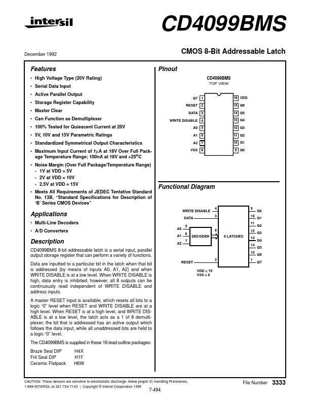
CD4099BMS 8-bit addressable latch is a serial input, parallel output storage register that can perform a variety of functions. Data are inputted to a particular bit in the latch when that bit is addressed (by means of inputs A0, A1, A2) and when WRITE DISABLE is at a low level. When WRITE DISABLE is high, data entry is inhibited; however, all 8 outputs can be continuously read independent of WRITE DISABLE and address inputs. A master RESET input is available, which resets all bits to a logic “0” level when RESET and WRITE DISABLE are at a high level. When RESET is at a high level, and WRITE DISABLE is at a low level, the latch acts as a 1 of 8 demultiplexer; the bit that is addressed has an active output which follows the data input, while all unaddressed bits are held to a logic “0” level. The CD4099BMS is supplied in these 16-lead outline packages: Braze Seal DIP Frit Seal DIP Ceramic Flatpack H4X H1F H6W A2 RESET VDD = 16 VSS = 8 CAUTION: These devices are sensitive to electrostatic discharge; follow proper IC Handling Procedures....