Datasheet Details
| Part number | MAX9160 |
|---|---|
| Manufacturer | Maxim |
| File Size | 348.22 KB |
| Description | LVDS or LVTTL/LVCMOS Input to 14 LVTTL/LVCMOS Output Clock Driver |
| Datasheet |
 MAX9160_MaximIntegratedProducts.pdf MAX9160_MaximIntegratedProducts.pdf
|
| Part number | MAX9160 |
|---|---|
| Manufacturer | Maxim |
| File Size | 348.22 KB |
| Description | LVDS or LVTTL/LVCMOS Input to 14 LVTTL/LVCMOS Output Clock Driver |
| Datasheet |
MAX9160_MaximIntegratedProducts.pdf
|
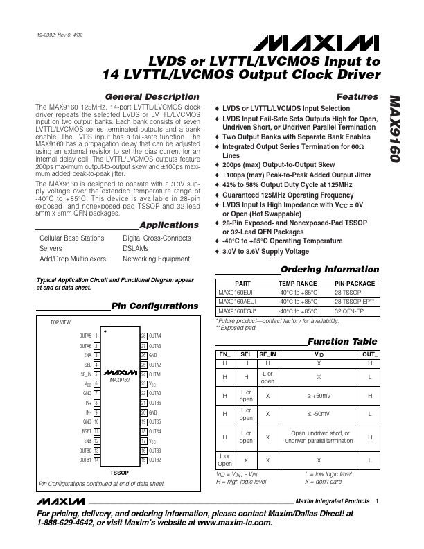
The MAX9160 125MHz, 14-port LVTTL/LVCMOS clock driver repeats the selected LVDS or LVTTL/LVCMOS input on two output banks.
📁 MAX9160 Similar Datasheet