Description
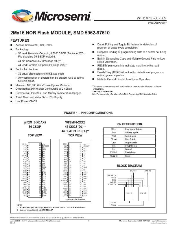
I/O0-15 A0-20 WE# CS1-2# OE# VCC VSS RY/BY# RESET#
Data Inputs/Outputs Address Inputs Write Enable Chip Select Output Enable Power Supply Ground Ready/Busy Reset
BLOCK DIAGRAM
I/O0-7
I/O8-15
RESET# WE# OE#
A0-20 RY/BY#
2M x 8
2M x 8
CS1# CS2#
Microsemi Corporation
(602) 437-1520
www.whiteedc.com www.microsemi.com
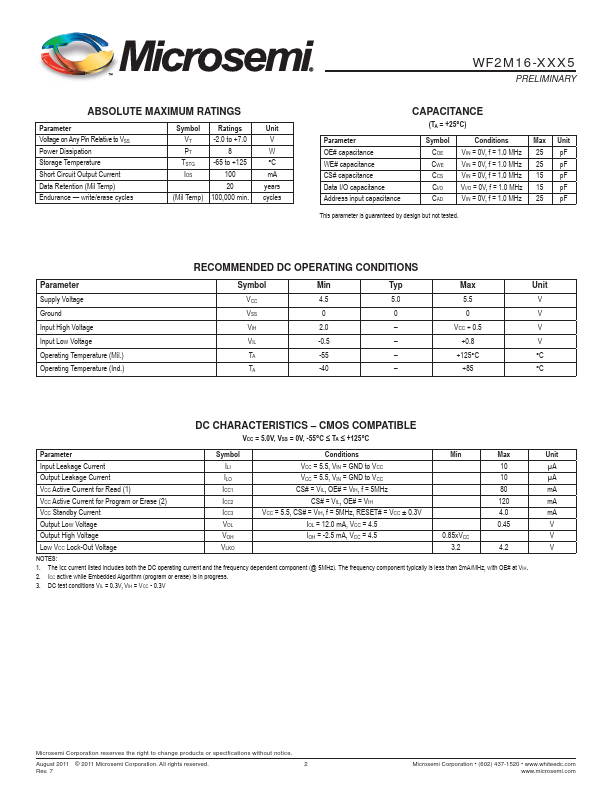
ABSOLUTE MAXIMUM RATINGS
Parameter Voltage on Any Pin Relative to VSS Power Dissipation Storage Temperature Short Circuit Output Current Data Retention (
Features
- Access Times of 90, 120, 150ns.
- Packaging:.
- 56 lead, Hermetic Ceramic, 0.520" CSOP (Package 207). Fits standard 56 SSOP footprint.
- 44 pin Ceramic SOJ (Package 102).
- 44 lead Ceramic Flatpack (Package 208).
- Sector Architecture.
- 32 equal size sectors of 64KBytes each.
- Any combination of sectors can be erased. Also supports full chip erase.
- Minimum 100,000 Write/Erase Cycles Minimum.
- Organized as 2Mx16;.
 WF2M16-XXX5-Microsemi.pdf