Description
Absolute Maximum Ratings
Supply Voltage (Vd) Supply Current (Id) Gate Bias Voltage (Vg) Input Power (Pin) Storage Temperature (Tstg) Operating Temperature (Ta) Channel Temperature (Tch)
+10.0 VDC 150 mA +0.3 VDC +18 dBm -65 to +165 OC -55 to MTTF Table 2 MTTF Table 2
(2) Channel temperature affects a device's MTTF.It is recommended to keep channel temperature as low as possible for maximum life.Electrical Characteristics (Ambient Temperature T = 25 oC)
Parameter Frequency Range (f ) Input R
Features
- Wide Band Driver Amplifier 9.0 dB Small Signal Gain 5.0 dB Noise Figure 15.0 dB Gain Control +9.0 dBm P1dB Compression Point 100% On-Wafer RF, DC and Output Power Testing 100% Visual Inspection to MIL-STD-883 Method 2010
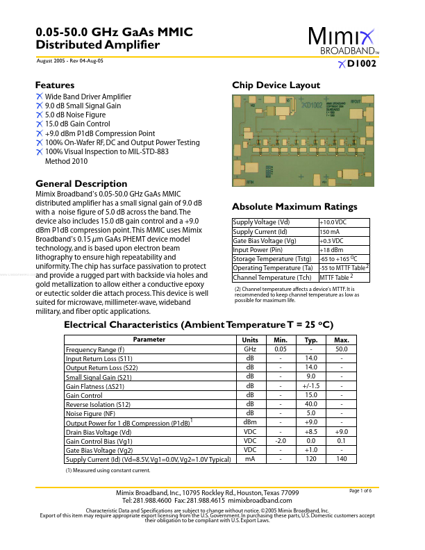
Chip Device Layout
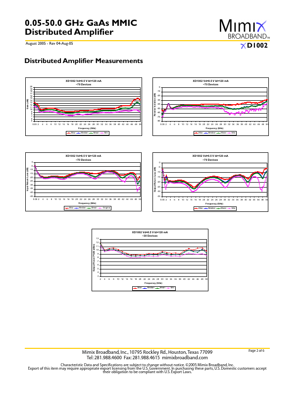
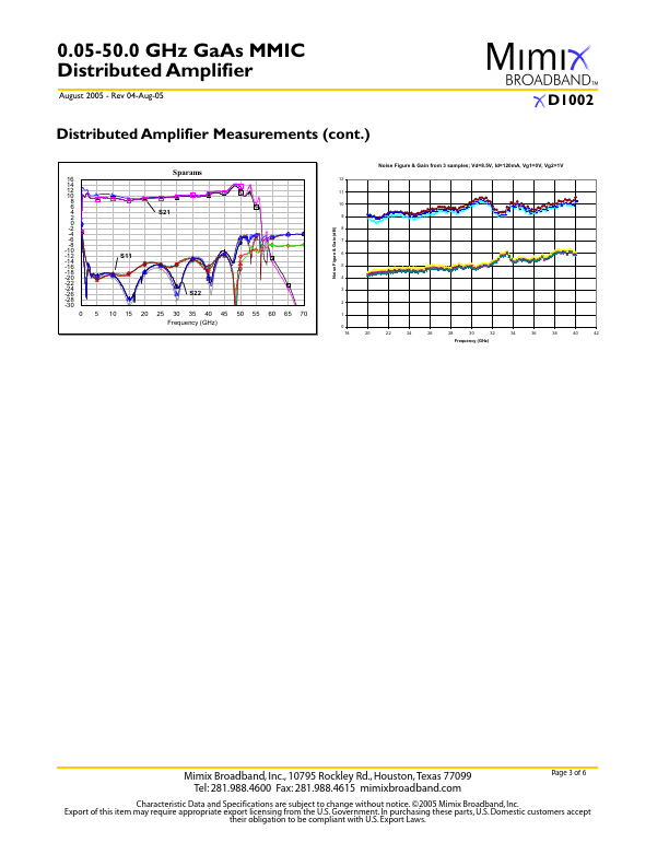
Mimix Broadband’s 0.05-50.0 GHz GaAs MMIC distributed amplifier has a small signal gain of 9.0 dB with a noise figure of 5.0 dB across the band. The device also includes 15.0 dB gain control and a +9.0 dBm P1dB compression point. This MMIC uses Mimix Broadba.
 XD1002_MimixBroadband.pdf