Description
Absolute Maximum Ratings
Supply Voltage (Vd) Supply Current (Id) Input Power (Pin) Storage Temperature (Tstg) Operating Temperature (Ta) Channel Temperature (Tch)
+6.0 VDC 270 mA +17.0 dBm -65 to +165 OC 1 -55 to MTTF Table 1 MTTF Table
(1) Channel temperature affects a device's MTTF.It is recommended to keep channel temperature as low as possible for maximum life.Electrical Characteristics (Ambient Temperature T = 25 oC)
Parameter
Frequency Range (f ) Input Return Loss (S11) Output Return
Features
- Ultra Wide Band Driver Amplifier Self Bias Architecture 23.0 dB Small Signal Gain 5.0 dB Noise Figure 100% On-Wafer RF, DC and Output Power Testing 100% Visual Inspection to MIL-STD-883 Method 2010
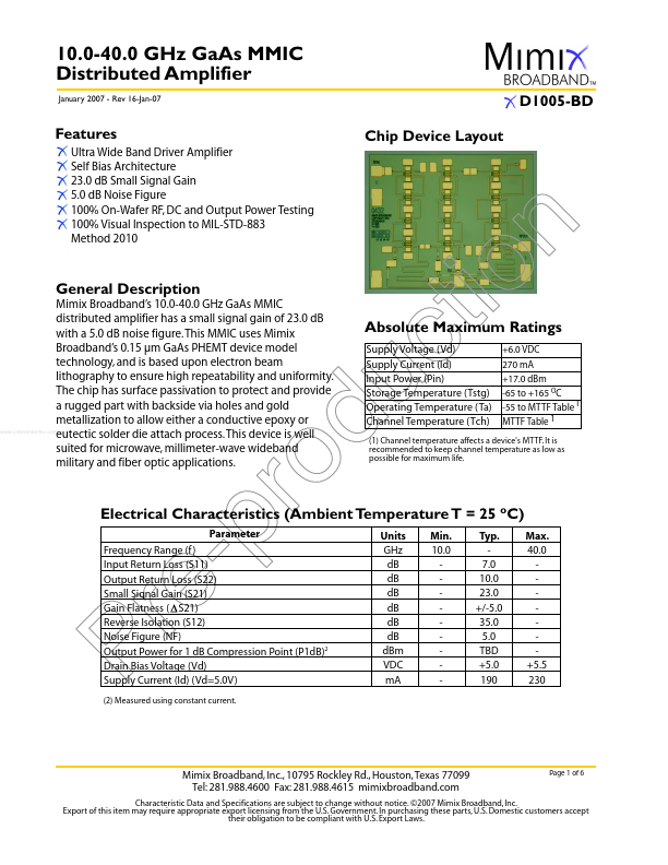
Chip Device Layout
Mimix Broadband’s 10.0-40.0 GHz GaAs MMIC distributed amplifier has a small signal gain of 23.0 dB with a 5.0 dB noise figure. This MMIC uses Mimix Broadband’s 0.15 µm GaAs PHEMT device model technology, and is based upon electron beam lithography to ensure high repeatability and.
 XD1005-BD_MimixBroadband.pdf