Description
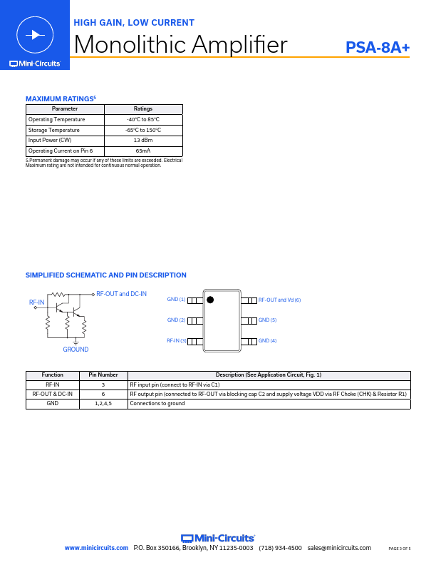
RF-IN
RF-OUT and DC-IN
GND (1)
GND (2)
GROUND
RF-IN (3)
RF-OUT and Vd (6) GND (5) GND (4)
Function RF-IN
RF-OUT & DC-IN GND
Pin Number 3 6
1,2,4,5
Description (See Application Circuit, Fig.1) RF input pin (connect to RF-IN via C1) RF output pin (connected to RF-OUT via blocking cap C2 and supply voltage VDD via RF Choke (CHK) & Resistor R1) Connections to ground
www.minicircuits.com P.O.Box 350166, Brooklyn, NY 11235-0003 (718) 934-4500 sales@minicircuits.com
PAGE 3 OF 5
HIGH GAIN
Features
- Feature
High Gain, 31 dB typ. at 0.1GHz
Advantages Enables signal amplification without the need for multiple gain stages. Low Noise, 3.0 dB typ. at 0.1GHz
Enables lower system noise figure performance. Low NF and High Gain results in lower NF systems
SOT-363 Package
Tiny footprint saves space in dense layouts while providing low inductance, repeatable transitions, and excellent thermal contact to the PCB. REV. A ECO-011279 PSA-8A+ MCL NY 220105
www. minicircuits. com P. O. Box 350166, Brook.

 PSA-8A+-Mini-Circuits.pdf