Datasheet Details
| Part number | MC68HC68R1 |
|---|---|
| Manufacturer | Motorola |
| File Size | 81.25 KB |
| Description | 8-BIT SERIAL STATIC RAMs |
| Datasheet |
 MC68HC68R1-Motorola.pdf MC68HC68R1-Motorola.pdf
|
| Part number | MC68HC68R1 |
|---|---|
| Manufacturer | Motorola |
| File Size | 81.25 KB |
| Description | 8-BIT SERIAL STATIC RAMs |
| Datasheet |
MC68HC68R1-Motorola.pdf
|
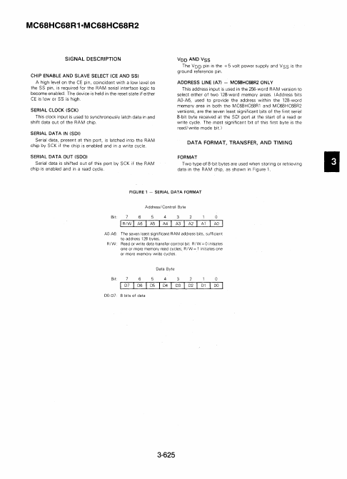
CHIP ENABLE AND SLAVE SELECT (CE AND SS) A high level on the CE pin, coincident with a low level on the SS pin, is required for the RAM serial interface logic to become enabled.The device is held in the reset state if either CE is low or SS is high.SERIAL CLOCK (SCK) This clock input is used to synchronously latch data in and shift data out of the RAM chip.SERIAL DATA IN (SDI) Serial data, present at this port, is latched into the RAM chip by SCK if the chip is enabled and in a write cycle.S
📁 MC68HC68R1 Similar Datasheet