Datasheet Details
| Part number | MPC9600 |
|---|---|
| Manufacturer | Motorola |
| File Size | 365.84 KB |
| Description | LOW VOLTAGE 2.5 V AND 3.3 V CMOS PLL CLOCK DRIVER |
| Datasheet |
 MPC9600 Datasheet MPC9600 Datasheet
|
|
|
| Part number | MPC9600 |
|---|---|
| Manufacturer | Motorola |
| File Size | 365.84 KB |
| Description | LOW VOLTAGE 2.5 V AND 3.3 V CMOS PLL CLOCK DRIVER |
| Datasheet |
MPC9600 Datasheet
|
|
|
|
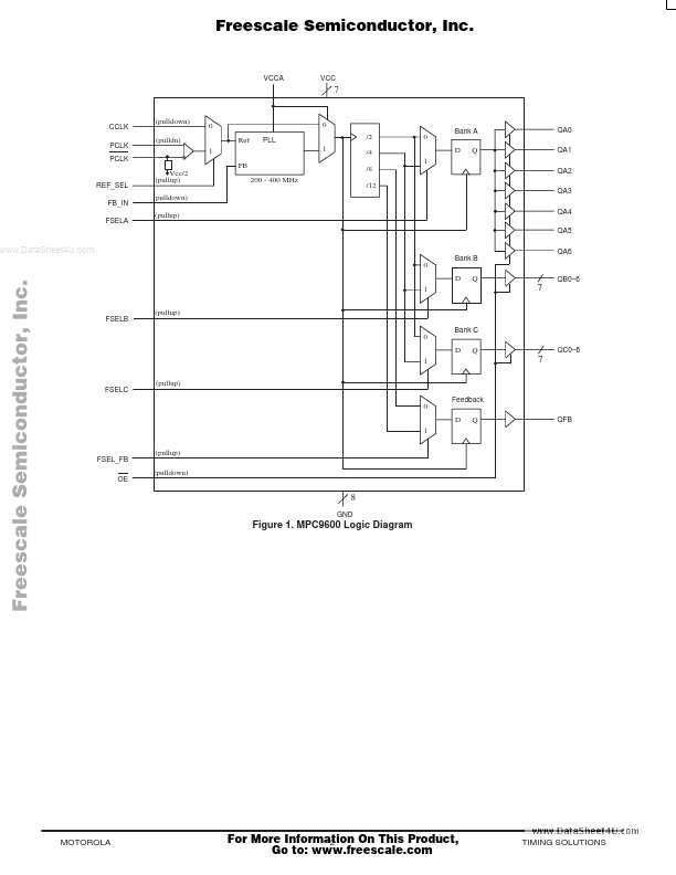
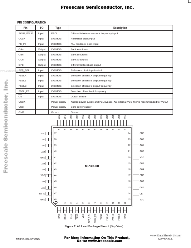
Differential reference clock frequency input Reference clock input PLL feedback clock input Bank A outputs Bank B outputs Bank C outputs Differential feedback output Reference clock input select Selection of bank A output frequency Selection of bank B output frequency Selection of bank C output frequency Selection of feedback frequency Output enable Analog power supply and PLL bypass.
📁 Similar Datasheet