Datasheet Details
| Part number | 74ABT32 |
|---|---|
| Manufacturer | NXP ↗ |
| File Size | 94.50 KB |
| Description | Quad 2-input OR gate |
| Datasheet |
 74ABT32_PhilipsSemiconductors.pdf 74ABT32_PhilipsSemiconductors.pdf
|
| Part number | 74ABT32 |
|---|---|
| Manufacturer | NXP ↗ |
| File Size | 94.50 KB |
| Description | Quad 2-input OR gate |
| Datasheet |
74ABT32_PhilipsSemiconductors.pdf
|
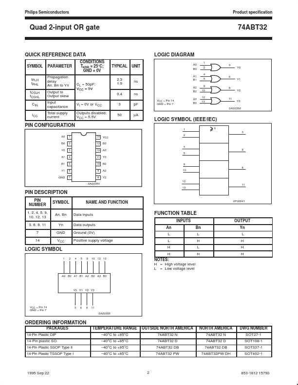
PIN NUMBER 1, 2, 4, 5, 9, 10, 12, 13 3, 6, 8, 11 7 14 SYMBOL An, Bn Yn GND VCC NAME AND FUNCTION Data inputs Data outputs Ground (0V) Positive supply voltage SF00041 FUNCTION TABLE INPUTS An L L H Bn L H L OUTPUT Yn L H H H LOGIC SYMBOL 1 2 4 5 9 10 12 13 H H NOTES: H = High voltage level L = Low voltage level A0 B0 A1 B1 A2 B2 A3 B3 Y0 Y1 Y2 Y3 VCC = Pin 14 GND = Pin 7 3 6 8 11 SA00355 ORDERING INFORMATION PACKAGES 14-Pin Plastic DIP 14-Pin plastic SO 14-Pin Plastic SSOP Type II 14-
📁 74ABT32 Similar Datasheet