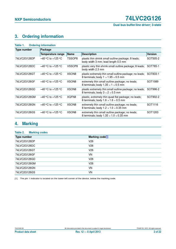
Datasheet Details
| Part number | 74LVC2G126 |
|---|---|
| Manufacturer | NXP |
| File Size | 172.50 KB |
| Description | Dual bus buffer/line driver |
| Datasheet |
 74LVC2G126 Datasheet 74LVC2G126 Datasheet
|
|
|
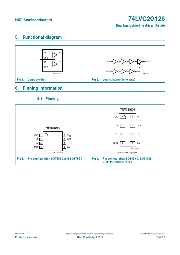
The 74LVC2G126 is a dual non-inverting buffer/line driver with 3-state outputs.
Each 3-state output is controlled by an output enable input (pin nOE).
A LOW-level at pin nOE causes the output to assume a high-impedance OFF-state.
| Part number | 74LVC2G126 |
|---|---|
| Manufacturer | NXP |
| File Size | 172.50 KB |
| Description | Dual bus buffer/line driver |
| Datasheet |
74LVC2G126 Datasheet
|
|
|
|