Datasheet4U Logo Datasheet4U.com

74LVC2G14 - Dual inverting Schmitt-trigger

Datasheet Summary

Description

APPLICATIONS 74LVC2G14 Wave and pulse shapers for highly noisy environments Astable multivibrators

Monostable multivibrators.

The 74LVC2G14 is a high-performance, low-power, low-voltage, Si-gate CMOS device and superior to most advanced CMOS compatible TTL families.

Features

  • Wide supply voltage range from 1.65 V to 5.5 V.
  • 5 V tolerant input/output for interfacing with 5 V logic.
  • High noise immunity.
  • Complies with JEDEC standard:.
  • JESD8-7 (1.65 V to 1.95 V).
  • JESD8-5 (2.3 V to 2.7 V).
  • JESD8B/JESD36 (2.7 V to 3.6 V).
  • ±24 mA output drive (VCC = 3.0 V).
  • CMOS low power consumption.
  • Latch-up performance exceeds 250 mA.
  • Direct interface with TTL levels.
  • Mulltiple pa.

📥 Download Datasheet

Datasheet preview – 74LVC2G14

Datasheet Details

Part number 74LVC2G14
Manufacturer NXP
File Size 97.26 KB
Description Dual inverting Schmitt-trigger
Datasheet download datasheet 74LVC2G14 Datasheet
Additional preview pages of the 74LVC2G14 datasheet.
Other Datasheets by NXP

Full PDF Text Transcription

Click to expand full text
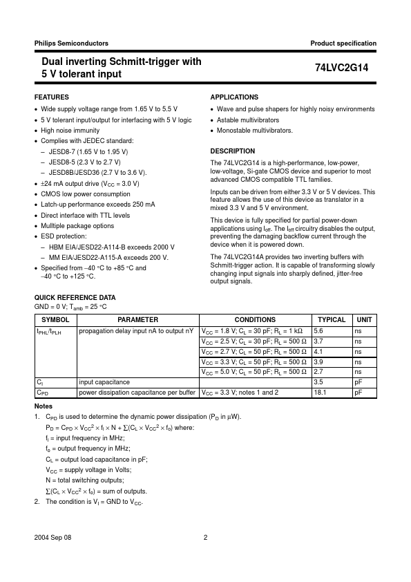
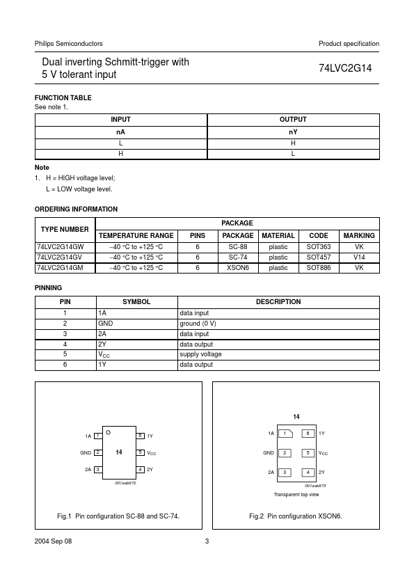
INTEGRATED CIRCUITS DATA SHEET 74LVC2G14 Dual inverting Schmitt-trigger with 5 V tolerant input Product specification Supersedes data of 2003 Jul 31 2004 Sep 08 Philips Semiconductors Product specification Dual inverting Schmitt-trigger with 5 V tolerant input FEATURES • Wide supply voltage range from 1.65 V to 5.5 V • 5 V tolerant input/output for interfacing with 5 V logic • High noise immunity • Complies with JEDEC standard: – JESD8-7 (1.65 V to 1.95 V) – JESD8-5 (2.3 V to 2.7 V) – JESD8B/JESD36 (2.7 V to 3.6 V). • ±24 mA output drive (VCC = 3.0 V) • CMOS low power consumption • Latch-up performance exceeds 250 mA • Direct interface with TTL levels • Mulltiple package options • ESD protection: – HBM EIA/JESD22-A114-B exceeds 2000 V – MM EIA/JESD22-A115-A exceeds 200 V.
Published: |