Datasheet Details
| Part number | 54F273 |
|---|---|
| Manufacturer | National Semiconductor |
| File Size | 363.35 KB |
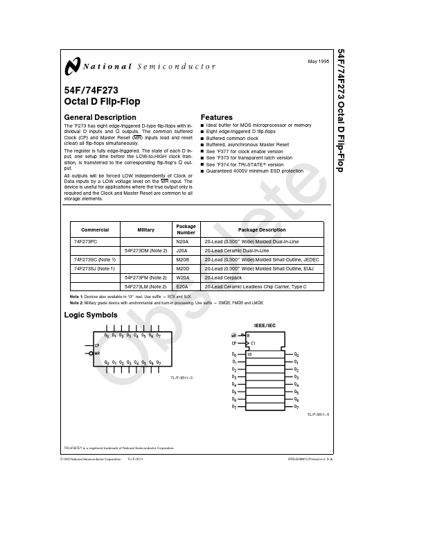
| Description | Octal D Flip-Flop |
| Datasheet |
 54F273 Datasheet 54F273 Datasheet
|
|
|
| Part number | 54F273 |
|---|---|
| Manufacturer | National Semiconductor |
| File Size | 363.35 KB |
| Description | Octal D Flip-Flop |
| Datasheet |
54F273 Datasheet
|
|
|
|