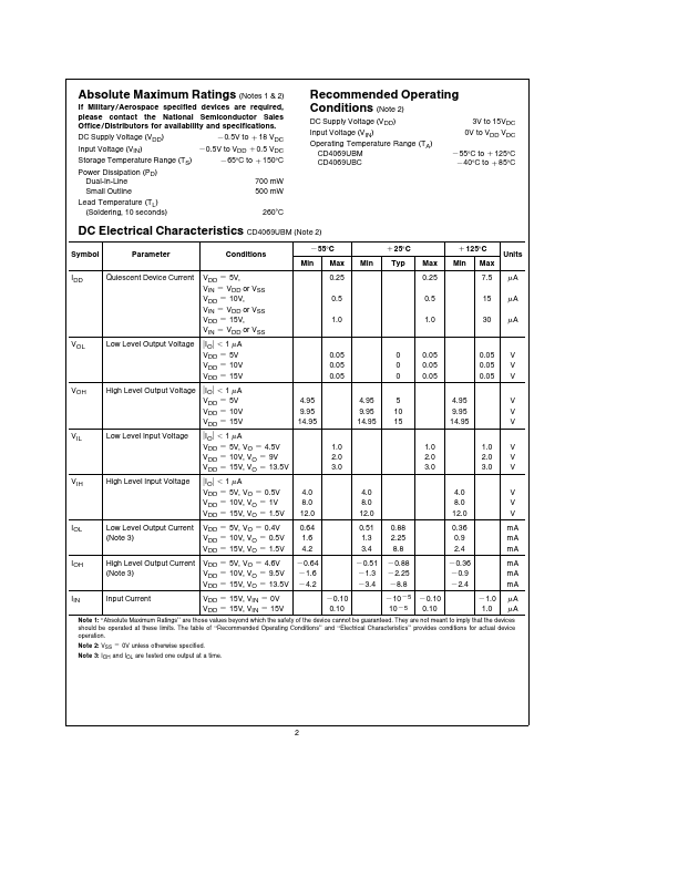
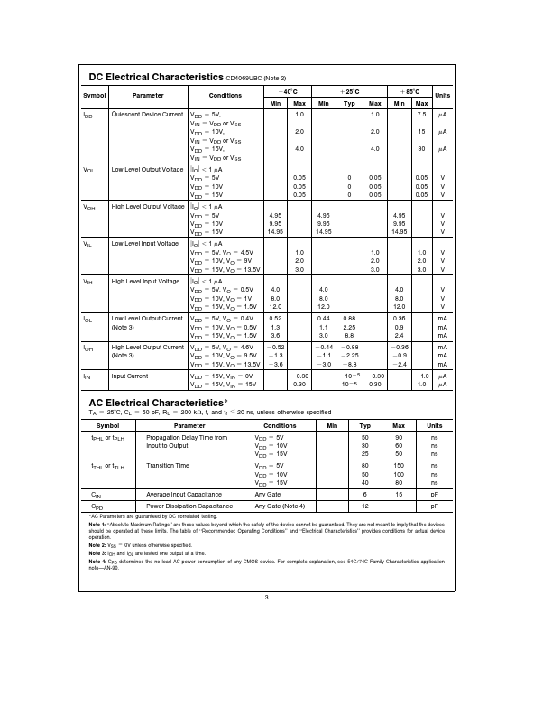
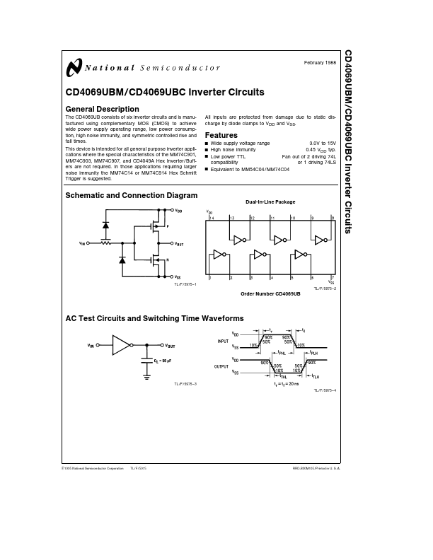
Datasheet4U Logo Datasheet4U.com

CD4069UBC - Inverter Circuits

Description

The CD4069UB consists of six inverter circuits and is manufactured using complementary MOS (CMOS) to achieve wide power supply operating range low power consumption high noise immunity and symmetric controlled rise and fall times This device is intended for all general purpose inverter applications

Features

  • Y Y Y Y Wide supply voltage range 3 0V to 15V High noise immunity 0 45 VDD typ Low power TTL Fan out of 2 driving 74L compatibility or 1 driving 74LS Equivalent to MM54C04 MM74C04 Schematic and Connection Diagram Dual-In-Line Package TL F 5975.
  • 1 TL F 5975.
  • 2 Order Number CD4069UB AC Test Circuits and Switching Time Waveforms TL F 5975.
  • 3 TL F 5975.
  • 4 C1995 National Semiconductor Corporation TL F 5975 RRD-B30M105 Printed in U S A Absolute Maximum Ra.

📥 Download Datasheet

Datasheet preview – CD4069UBC
Other Datasheets by National Semiconductor

Full PDF Text Transcription

Click to expand full text
CD4069UBM CD4069UBC Inverter Circuits February 1988 CD4069UBM CD4069UBC Inverter Circuits General Description The CD4069UB consists of six inverter circuits and is manufactured using complementary MOS (CMOS) to achieve wide power supply operating range low power consumption high noise immunity and symmetric controlled rise and fall times This device is intended for all general purpose inverter applications where the special characteristics of the MM74C901 MM74C903 MM74C907 and CD4049A Hex Inverter Buffers are not required In those applications requiring larger noise immunity the MM74C14 or MM74C914 Hex Schmitt Trigger is suggested All inputs are protected from damage due to static discharge by diode clamps to VDD and VSS Features Y Y Y Y Wide supply voltage range 3 0V to 15V High nois
Published: |