Description
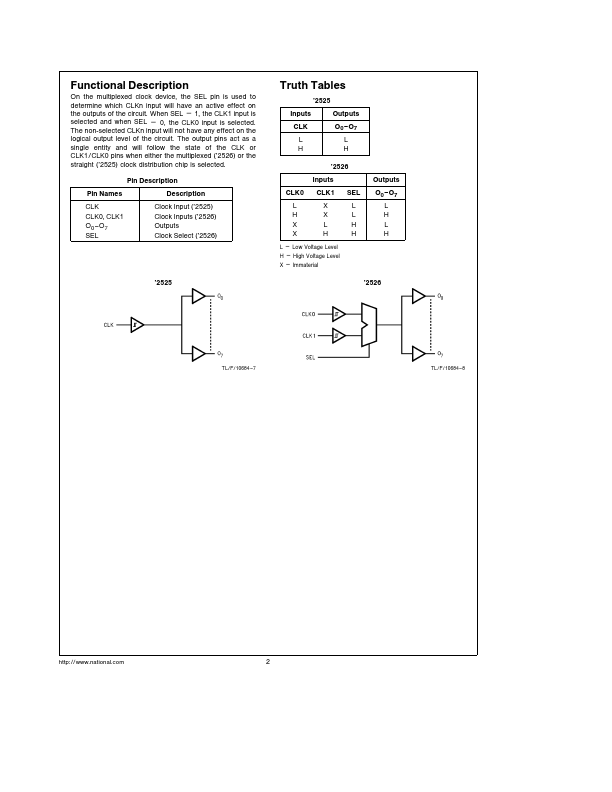
On the multiplexed clock device the SEL pin is used to determine which CLKn input will have an active effect on the outputs of the circuit When SEL e 1 the CLK1 input is selected and when SEL e 0 the CLK0 input is selected The non-selected CLKn input will not have any effect on the logical output level of the circuit The output pins act as a single entity and will follow the state of the CLK or CLK1 CLK0 pins when either the multiplexed (’2526) or the straight (’2525) clock distribution chip is
Features
- Y These CGS devices implement National’s FACTTM family
Y Ideal for signal generation and clock distribution Y Guaranteed pin to pin and part to part skew Y Multiplexed clock input (’2526) Y Guaranteed 2 kV minimum ESD protection Y Symmetric output current drive of 24 mA for IOL IOH Y ’CT has TTL-compatible inputs Y These products are identical to 74AC ACT2525 and
2526 Y Available as Mil Aero versions
54AC ACT2525 54AC ACT2526
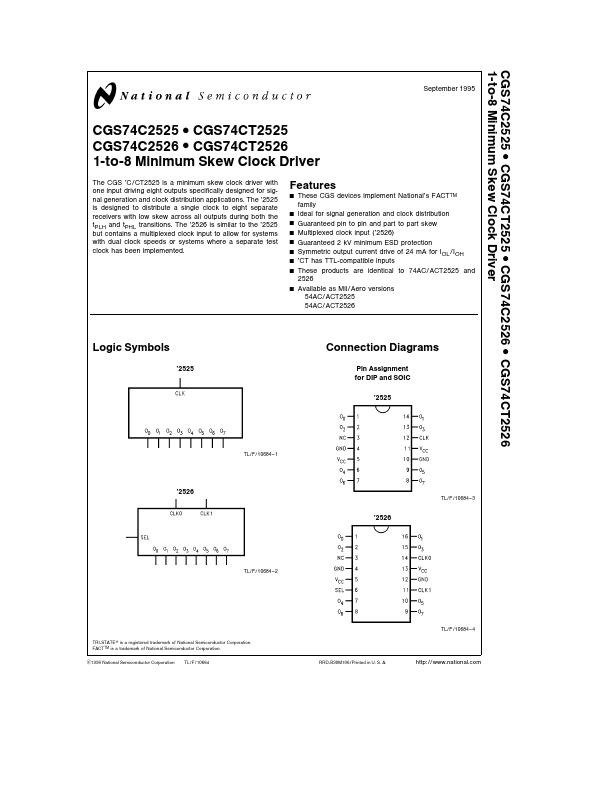
Logic Symbols
’2525
Connection Diagrams
Pin Assignment for DIP and S.
 CGS74CT2526_NationalSemiconductor.pdf