DM7474
Overview
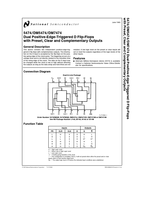
This device contains two independent positive-edge-triggered D flip-flops with complementary outputs The information on the D input is accepted by the flip-flops on the positive going edge of the clock pulse The triggering occurs at a voltage level and is not directly related to the transition time of the rising edge of the clock The data on the D input may be changed while the clock is low or high without affecting the outputs as long as the data setup and hold times are not violated A low logic level on the preset or clear inputs will set or reset the outputs regardless of the logic levels of the other inputs.